- 您現(xiàn)在的位置:買賣IC網(wǎng) > PDF目錄30743 > LM1881MX-X/NOPB (NATIONAL SEMICONDUCTOR CORP) SYNC SEPARATOR IC, PDSO8 PDF資料下載
參數(shù)資料
| 型號: | LM1881MX-X/NOPB |
| 廠商: | NATIONAL SEMICONDUCTOR CORP |
| 元件分類: | 信號分離 |
| 英文描述: | SYNC SEPARATOR IC, PDSO8 |
| 封裝: | PLASTIC, SO-8 |
| 文件頁數(shù): | 4/11頁 |
| 文件大?。?/td> | 275K |
| 代理商: | LM1881MX-X/NOPB |

Absolute Maximum Ratings (Note 1)
If Military/Aerospace specified devices are required,
please contact the National Semiconductor Sales Office/
Distributors for availability and specifications.
Supply Voltage
13.2V
Input Voltage
3 V
P-P (VCC = 5V)
6V
P-P (VCC ≥ 8V)
Output Sink Currents; Pins, 1, 3, 5
5 mA
Output Sink Current; Pin 7
2 mA
Package Dissipation (Note 2)
1100 mW
Operating Temperature Range
0C–70C
Storage Temperature Range
65C to +150C
ESD Susceptibility (Note 3)
2 kV
Soldering Information
Dual-In-Line Package (10 sec.)
260C
Small Outline Package
Vapor Phase (60 sec.)
215C
Infrared (15 sec.)
220C
See AN-450 “Surface Mounting Methods and their Effect
on Product Reliability” for other methods of soldering
surface mount devices.
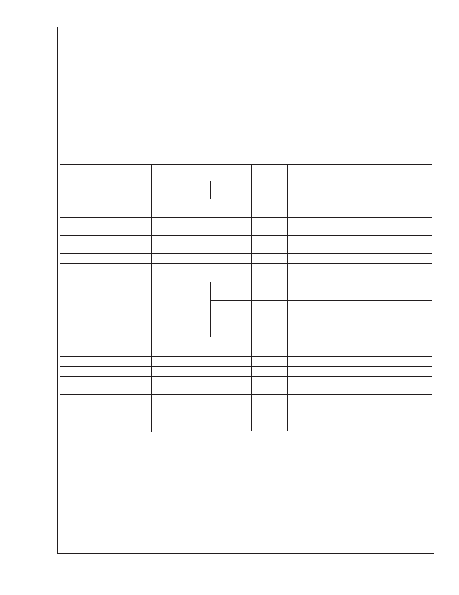
Electrical Characteristics
V
CC = 5V; RSET = 680 k;TA = 25C; Unless otherwise specified
Parameter
Conditions
Typ
Tested
Limit (Note 4)
Design
Limit (Note 5)
Units
(Limits)
Supply Current
Outputs at
Logic 1
V
CC =5V
V
CC = 12V
5.2
5.5
10
12
mAmax
DC Input Voltage
Pin 2
1.5
1.3
1.8
Vmin
Vmax
Input Threshold Voltage
(Note 6)
70
55
85
mVmin
mVmax
Input Discharge Current
Pin 2; V
IN =2V
11
6
16
Amin
Amax
Input Clamp Charge Current
Pin 2; V
IN = 1V
0.8
0.2
mAmin
R
SET Pin Reference Voltage
Pin 6; (Note 7)
1.22
1.10
1.35
Vmin
Vmax
Composite Sync. & Vertical
Outputs
I
OUT =40A;
Logic 1
V
CC =5V
V
CC = 12V
4.5
4.0
11.0
Vmin
I
OUT = 1.6 mA
Logic 1
V
CC =5V
V
CC = 12V
3.6
2.4
10.0
Vmin
Burst Gate & Odd/Even
Outputs
I
OUT =40A;
Logic 1
V
CC =5V
V
CC = 12V
4.5
4.0
11.0
Vmin
Composite Sync. Output
I
OUT = 1.6 mA; Logic 0; Pin 1
0.2
0.8
Vmax
Vertical Sync. Output
I
OUT = 1.6 mA; Logic 0; Pin 3
0.2
0.8
Vmax
Burst Gate Output
I
OUT = 1.6 mA; Logic 0; Pin 5
0.2
0.8
Vmax
Odd/Even Output
I
OUT = 1.6 mA; Logic 0; Pin 7
0.2
0.8
Vmax
Vertical Sync Width
230
190
300
smin
smax
Burst Gate Width
2.7 k
from Pin 5 to V
CC
4
2.5
4.7
smin
smax
Vertical Default Time
(Note 8)
65
32
90
smin
smax
Note 1: Absolute Maximum Ratings indicate limits beyond which damage to the device may occur. Operating Ratings indicate conditions for which the device is
functional, but do not guarantee specific performance limits. For guaranteed specifications and test conditions, see the Electrical Characteristics. The guaranteed
specifications apply only for the test conditions listed. Some performance characteristics may degrade when the device is not operated under the listed test
conditions.
Note 2: For operation in ambient temperatures above 25C, the device must be derated based on a 150C maximum junction temperature and a package thermal
resistance of 110C/W, junction to ambient.
Note 3: ESD susceptibility test uses the “human body model, 100 pF discharged through a 1.5 k
resistor”.
Note 4: Typicals are at TJ = 25C and represent the most likely parametric norm.
Note 5: Tested Limits are guaranteed to National’s AOQL (Average Outgoing Quality Level).
Note 6: Relative difference between the input clamp voltage and the minimum input voltage which produces a horizontal output pulse.
Note 7: Careful attention should be made to prevent parasitic capacitance coupling from any output pin (Pins 1, 3, 5 and 7) to the RSET pin (Pin 6).
Note 8: Delay time between the start of vertical sync (at input) and the vertical output pulse.
LM1881
www.national.com
2
相關PDF資料 |
PDF描述 |
|---|---|
| LM1881N-X/NOPB | SYNC SEPARATOR IC, PDIP8 |
| LM1882-RCMX | SPECIALTY CONSUMER CIRCUIT, PDSO20 |
| 54ACT715-RD | SPECIALTY CONSUMER CIRCUIT, CDIP20 |
| 54ACT715D | SPECIALTY CONSUMER CIRCUIT, CDIP20 |
| 54ACT715-RLX | SPECIALTY CONSUMER CIRCUIT, CQCC20 |
相關代理商/技術參數(shù) |
參數(shù)描述 |
|---|---|
| LM1881N | 功能描述:視頻 IC RoHS:否 制造商:Fairchild Semiconductor 工作電源電壓:5 V 電源電流:80 mA 最大工作溫度:+ 85 C 封裝 / 箱體:TSSOP-28 封裝:Reel |
| LM1881N | 制造商:Texas Instruments 功能描述:VIDEO SYNC SEPARATOR 1881 DIP8 |
| LM1881N/NOPB | 功能描述:視頻 IC RoHS:否 制造商:Fairchild Semiconductor 工作電源電壓:5 V 電源電流:80 mA 最大工作溫度:+ 85 C 封裝 / 箱體:TSSOP-28 封裝:Reel |
| LM1881N/NOPB | 制造商:Texas Instruments 功能描述:Special Function IC |
| LM1881N-8/NOPB | 制造商:Texas Instruments 功能描述: |
發(fā)布緊急采購,3分鐘左右您將得到回復。