- 您現(xiàn)在的位置:買賣IC網(wǎng) > PDF目錄358818 > LM2445TA (NATIONAL SEMICONDUCTOR CORP) Monolithic Triple 7.5 ns CRT Driver PDF資料下載
參數(shù)資料
| 型號: | LM2445TA |
| 廠商: | NATIONAL SEMICONDUCTOR CORP |
| 元件分類: | 音頻/視頻放大 |
| 英文描述: | Monolithic Triple 7.5 ns CRT Driver |
| 中文描述: | 3 CHANNEL, VIDEO AMPLIFIER, PZFM9 |
| 封裝: | PLASTIC, TO-220, 9 PIN |
| 文件頁數(shù): | 7/14頁 |
| 文件大小: | 758K |
| 代理商: | LM2445TA |

Application Hints
(Continued)
OPTIMIZING TRANSIENT RESPONSE
Referring to
Figure 9
, there are three components (R1, R2
and L1) that can be adjusted to optimize the transient re-
sponse of the application circuit. Increasing the values of R1
and R2 will slow the circuit down while decreasing over-
shoot. Increasing the value of L1 will speed up the circuit as
well as increase overshoot. It is very important to use induc-
tors with very high self-resonant frequencies, preferably
above 300 MHz. Ferrite core inductors from J.W. Miller
Magnetics (part
#
78FR--k) were used for optimizing the
performance of the device in the NSC application board. The
values shown in
Figure 11
and
Figure 12
can be used as a
good starting point for the evaluation of the LM2445. Using
variable resistors for R1 and the parallel resistor will simplify
finding the values needed for optimum performance in a
given application. Once the optimum values are determined
the variable resistors can be replaced with fixed values.
EFFECT OF LOAD CAPACITANCE
Figure 8
shows the effect of increased load capacitance on
the speed of the device. This demonstrates the importance
of knowing the load capacitance in the application.
EFFECT OF OFFSET
Figure 7
shows the variation in rise and fall times when the
output offset of the device is varied from 40 to 50 V
. The
rise time shows a maximum variation relative to the center
data point (45 V
) less than 5%. The fall time shows a
variation of less than 8% relative to the center data point.
THERMAL CONSIDERATIONS
Figure 4
shows the performance of the LM2445 in the test
circuit shown in
Figure 2
as a function of case temperature.
The figure shows that the rise time of the LM2445 increases
by approximately 10% as the case temperature increases
from 50C to 100C. This corresponds to a speed degrada-
tion of 2% for every 10C rise in case temperature. The fall
time increases by approximately 7% as the case tempera-
ture increases from 50C to 100C.
Figure 6
shows the maximum power dissipation of the
LM2445 vs. Frequency when all three channels of the device
are driving an 8 pF load with a 40 V
p-p
alternating one pixel
on, one pixel off signal. The graph assumes a 72% active
time (device operating at the specified frequency) which is
typical in a monitor application. The other 28% of the time
the device is assumed to be sitting at the black level (65V in
this case). This graph gives the designer the information
needed to determine the heat sink requirement for his appli-
cation. The designer should note that if the load capacitance
is increased the AC component of the total power dissipation
will also increase.
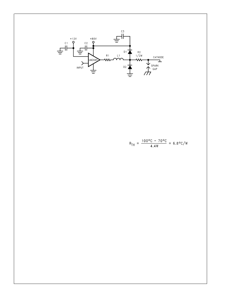
The LM2445 case temperature must be maintained below
100C. If the maximum expected ambient temperature inside
the monitor is 70C and the power dissipation is 4.4W (from
Figure 6
, 50 MHz max. video frequency), then a maximum
heat sink thermal resistance can be calculated:
This example assumes a capacitive load of 8 pF and no
resistive load.
TYPICAL APPLICATION
Atypical application of the LM2445 is shown in
Figure 11
and
Figure 12
. Used in conjunction with an LM1267, a complete
video channel from monitor input to CRT cathode can be
achieved. Performance is ideal for 1024 x 768 resolution
displays with pixel clock frequencies up to 95 MHz.
Figure 11
and
Figure 12
are the schematic for the NSC demonstration
board that can be used to evaluate the LM1267/2466 com-
bination in a monitor, and
Figure 10
shows the typical re-
sponse at the red cathode for this application. The input
video rise time is 3.2ns, and the peaking component values
are those recommended in
Figure 12
.
Table 1
shows the
typical cathode response of all three channels.
20063710
FIGURE 9. One Channel of the LM2445 with the Recommended Application Circuit
L
www.national.com
7
相關(guān)PDF資料 |
PDF描述 |
|---|---|
| LM2460 | Monolithic Triple Channel High Swing CRT Driver |
| LM2460TA | Monolithic Triple Channel High Swing CRT Driver |
| LM2462 | Monolithic Triple 3 ns CRT Driver |
| LM2462TA | Monolithic Triple 3 ns CRT Driver |
| LM2467TA | Monolithic Triple 7.5 ns CRT Driver |
相關(guān)代理商/技術(shù)參數(shù) |
參數(shù)描述 |
|---|---|
| LM2445TA/NOPB | 功能描述:IC DRIVER CRT 3CH 7.5NS 9-TO-220 RoHS:是 類別:集成電路 (IC) >> PMIC - 顯示器驅(qū)動(dòng)器 系列:- 產(chǎn)品培訓(xùn)模塊:Lead (SnPb) Finish for COTS Obsolescence Mitigation Program 標(biāo)準(zhǔn)包裝:2,500 系列:- 顯示器類型:真空熒光 (VF) 配置:5 x 7(矩陣) 接口:串行 數(shù)字或字符:- 電流 - 電源:3.5mA 電源電壓:2.7 V ~ 3.6 V 工作溫度:-40°C ~ 125°C 安裝類型:表面貼裝 封裝/外殼:16-SSOP(0.154",3.90mm 寬) 供應(yīng)商設(shè)備封裝:16-QSOP 包裝:帶卷 (TR) |
| LM2450 | 制造商:NSC 制造商全稱:National Semiconductor 功能描述:220V Monolithic Triple Channel 7 MHz DC Coupled CRT DTV Driver |
| LM2451 | 制造商:NSC 制造商全稱:National Semiconductor 功能描述:220V Monolithic Triple Channel 12 MHz DC Coupled CRT DTV Driver |
| LM2451TB | 制造商:Rochester Electronics LLC 功能描述: 制造商:Texas Instruments 功能描述: |
| LM2451TB/NOPB | 功能描述:顯示驅(qū)動(dòng)器和控制器 RoHS:否 制造商:Panasonic Electronic Components 工作電源電壓:2.7 V to 5.5 V 最大工作溫度: 安裝風(fēng)格:SMD/SMT 封裝 / 箱體:QFN-44 封裝:Reel |
發(fā)布緊急采購,3分鐘左右您將得到回復(fù)。