- 您現(xiàn)在的位置:買賣IC網(wǎng) > PDF目錄385477 > LM2647LQX (NATIONAL SEMICONDUCTOR CORP) Dual Synchronous Buck Regulator Controller PDF資料下載
參數(shù)資料
| 型號: | LM2647LQX |
| 廠商: | NATIONAL SEMICONDUCTOR CORP |
| 元件分類: | 穩(wěn)壓器 |
| 英文描述: | Dual Synchronous Buck Regulator Controller |
| 中文描述: | DUAL SWITCHING CONTROLLER, 345 kHz SWITCHING FREQ-MAX, QCC28 |
| 封裝: | LLP-28 |
| 文件頁數(shù): | 18/25頁 |
| 文件大小: | 763K |
| 代理商: | LM2647LQX |
Application Information
(Continued)
The case of a single input capacitor supplying two channels
running out of phase is now discussed in detail and it shows
how to formally calculate the input RMS current capability
required. The example represents a very general case in
terms of the output voltages simply to highlight the various
possible applications of the LM2647 other than its primary
intended application. One of the most important questions to
answer here is: what input voltage really gives the worst
possible (highest) input RMS current This information is
required to size the capacitor correctly.
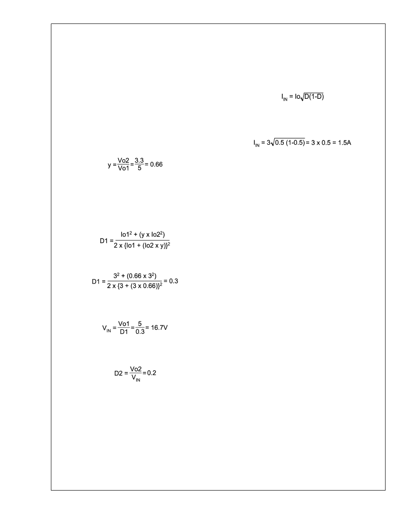
Example:
Consider two channels running at 5V
@
3A and
3.3V
@
3A. What is the worst case input capacitor RMS cur-
rent if the input varies from 10V to 28V
Step1:
Call the output with the higher voltage as Vo1 and the
other as Vo2. Then find the ratio ‘y’ as shown below
y is clearly going to be equal to or less than 1 by definition
(since Vo2
≤
Vo1). This step is required for using the equa-
tion presented in the next step.
Step2:
The equation for the input current has been derived
and it reveals that the worst-case occurs when the duty cycle
of the first channel is
where ‘y’ has been defined in Step 1. So
Therefore the appropriate input voltage to calculate the
worst case RMS input current is
Step3:
Calculate the duty cycle of the other channel when
this happens
Step4:
Calculate input capacitor RMS current by using the
known equation
I
IN2
= (Io1
2
D1) + (Io2
2
D2) - [Iol
D1+Io2
D2]
2
I
IN2
= (3
2
0.3) + (3
2
0.2) - [(3
0.3) + (3
0.2)]
2
Solving
I
IN
= 1.5A
Step5:
But what is really the worst case
It may have simply concluded at this point that "the rating of
the input capacitor must be greater or equal than 1.5A,
otherwise the life/reliability of the capacitor may be affected
severely etc.".And that is true but only under the single-point
load conditions used for the calculation. It will now be seen
that the worst case may still have gone unrecognized! What
if maximum load currents are not being drawn simulta-
neously as was assumed in our example It can be shown
that the capacitor could actually see higher currents than
calculated in Step 4.
Suppose one channel was completely unloaded. So in effect
there is only a single output of 5V
@
3A. The equation for the
RMS current through the input capacitor is then
The function D(1-D) has a maxima at D = 0.5. This would
correspond to an input voltage of 5V/0.5 = 10V.And the input
capacitor current at this worst case input voltage would be
It is just a coincidence in this application that in both cases
(above and at the end of Step 4) we have calculated the
same RMS current rating for the capacitor. In general, Step
4 can certainly yield smaller values than those for a single
channel, and this may mislead us into an improper selection
of the input capacitor. It must be remembered that Step 4 is
not necessarily the worst case. We must always take the
higher of the two values so calculated.
Incidentally, the above method for a single channel is also
the method to be used to calculate the capacitor rating when
the LM2647 is formally used for single channel operation, or
if both channels are being used but separate input capaci-
tors are being allocated for each channel.
In all cases the input capacitors must be positioned physi-
cally close to their respective stages. But if separate input
capacitors are being used for each channel, the input traces
to the two inputs must be long and thin so as to introduce a
measure of high frquency decoupling between the now
separated stages.
The designer may ask, what is the use of interleaved switch-
ing if the result of the interleaved calculation in Step 4 may
not even be used in our particular example Interleaved
switching certainly reduces cost because if the calculation
had been carried out for two non-interleaved channels
(switching in phase), both delivering maximum load, the
capacitor RMS current would have been much higher.
Note that the equations used in the above sections apply
only if the duty cycles of both channels are less than or equal
to 50% (and there is therefore no overlap in the current
waveforms). The equations for overlapping waveforms are
out of scope here.
MOSFETs
The selection of the MOSFETS should be done carefully to
maximize both efficiency and reliability together. There is a
different set of criteria for selecting the upper FET and lower
FET. It will also be seen that using very fast FETs without
deliberate thought, may seem to improve efficiency dramati-
cally on one prototype board but can impair efficiency on
another apparently ‘identical’ board, specially at light loads.
Therefore, the quest for improved efficiency must be
weighed against the possible penalty for doing this without
deeper understanding of the nuances of synchronous
switching buck stages in general. The criteria for selection
are briefly:
a) The upper FET is chosen basically for high switching
speed because in a typical synchronous buck regulator only
L
www.national.com
18
相關(guān)PDF資料 |
PDF描述 |
|---|---|
| LM2647MTC | Dual Synchronous Buck Regulator Controller |
| LM2665M6 | Switched Capacitor Voltage Converter |
| LM2665M6X | Switched Capacitor Voltage Converter |
| LM2707 | Inductive-Boost Series LED Driver with Programmable Oscillator Frequency |
| LM2707MF | Inductive-Boost Series LED Driver with Programmable Oscillator Frequency |
相關(guān)代理商/技術(shù)參數(shù) |
參數(shù)描述 |
|---|---|
| LM2647LQX/NOPB | 功能描述:DC/DC 開關(guān)控制器 RoHS:否 制造商:Texas Instruments 輸入電壓:6 V to 100 V 開關(guān)頻率: 輸出電壓:1.215 V to 80 V 輸出電流:3.5 A 輸出端數(shù)量:1 最大工作溫度:+ 125 C 安裝風(fēng)格: 封裝 / 箱體:CPAK |
| LM2647MTC | 功能描述:DC/DC 開關(guān)控制器 RoHS:否 制造商:Texas Instruments 輸入電壓:6 V to 100 V 開關(guān)頻率: 輸出電壓:1.215 V to 80 V 輸出電流:3.5 A 輸出端數(shù)量:1 最大工作溫度:+ 125 C 安裝風(fēng)格: 封裝 / 箱體:CPAK |
| LM2647MTC/NOPB | 功能描述:DC/DC 開關(guān)控制器 RoHS:否 制造商:Texas Instruments 輸入電壓:6 V to 100 V 開關(guān)頻率: 輸出電壓:1.215 V to 80 V 輸出電流:3.5 A 輸出端數(shù)量:1 最大工作溫度:+ 125 C 安裝風(fēng)格: 封裝 / 箱體:CPAK |
| LM2647MTCX | 功能描述:DC/DC 開關(guān)控制器 RoHS:否 制造商:Texas Instruments 輸入電壓:6 V to 100 V 開關(guān)頻率: 輸出電壓:1.215 V to 80 V 輸出電流:3.5 A 輸出端數(shù)量:1 最大工作溫度:+ 125 C 安裝風(fēng)格: 封裝 / 箱體:CPAK |
| LM2647MTCX/NOPB | 功能描述:DC/DC 開關(guān)控制器 RoHS:否 制造商:Texas Instruments 輸入電壓:6 V to 100 V 開關(guān)頻率: 輸出電壓:1.215 V to 80 V 輸出電流:3.5 A 輸出端數(shù)量:1 最大工作溫度:+ 125 C 安裝風(fēng)格: 封裝 / 箱體:CPAK |
發(fā)布緊急采購,3分鐘左右您將得到回復(fù)。