- 您現(xiàn)在的位置:買(mǎi)賣(mài)IC網(wǎng) > PDF目錄358828 > LM2710 (National Semiconductor Corporation) Step-up PWM DC/DC Converter Integrated with 5 Buffers PDF資料下載
參數(shù)資料
| 型號(hào): | LM2710 |
| 廠商: | National Semiconductor Corporation |
| 英文描述: | Step-up PWM DC/DC Converter Integrated with 5 Buffers |
| 中文描述: | 升壓PWM直流/直流轉(zhuǎn)換器內(nèi)建5緩沖器 |
| 文件頁(yè)數(shù): | 6/20頁(yè) |
| 文件大?。?/td> | 853K |
| 代理商: | LM2710 |
第1頁(yè)第2頁(yè)第3頁(yè)第4頁(yè)第5頁(yè)當(dāng)前第6頁(yè)第7頁(yè)第8頁(yè)第9頁(yè)第10頁(yè)第11頁(yè)第12頁(yè)第13頁(yè)第14頁(yè)第15頁(yè)第16頁(yè)第17頁(yè)第18頁(yè)第19頁(yè)第20頁(yè)

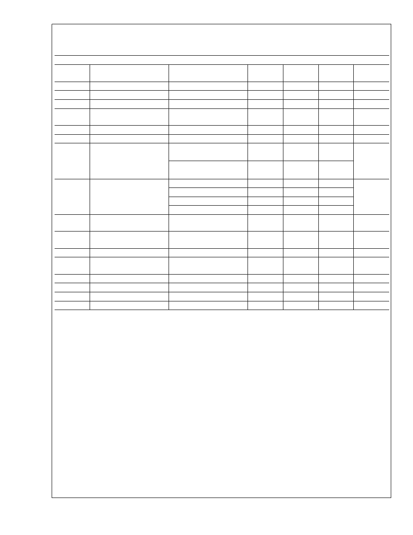
Electrical Characteristics
Specifications in standard type face are for T
= 25C and those with
boldface type
apply over the full
Operating Tempera-
ture Range
( T
J
= 40C to +125C). Unless otherwise specified, V
IN
=2.2V and Vs+ = 8V, Rox = 50
, Cox = 1nF.
BUFFERS
Symbol
Parameter
Conditions
Min
(Note 4)
Typ
(Note 5)
2.5
8
170
Max
(Note 4)
10
Units
V
OS
V
os
/
T
I
B
CMVR
Input offset voltage
Offset Voltage Drift
Input Bias Current
Input Common-mode Voltage
Range
Input Impedance
Input Capacitance
Continuous Output Current
mV
μV/C
nA
800
0.05
Vs+-0.05
V
Z
IN
C
IN
I
OUT
400
1
59
53
71
61
k
pF
Vs+=8V, Source
Vs+=8V, Sink
Vs+=12V, Source
Vs+=12V, Sink
R
L
=10k, Vo min.
R
L
=10k, Vo max.
R
L
=2k, Vo min.
R
L
=2k, Vo max.
R
L
=2 k
R
L
=10 k
R
L
=2 k
, Buffer input=0.5 to
(Vs+-0.5V)
41
65
50
75
71
36
85
42
0.075
mA
V
OUT
Swing
V
7.88
0.075
7.865
0.995
0.9985
A
VCL
Voltage Gain
0.998
0.9999
V/V
NL
Gain Linearity
0.01
%
Vs+
PSRR
Supply Voltage
Power Supply Rejection
Ratio
Supply Current/Amplifier
Slew Rate
Bandwidth
Phase Margin
4
12
V
Vs+ = 4 to 12V
90
316
μV/V
Is+
SR
BW
φ
0
Vo = Vs+/2, No Load
1
10
6
50
2
mA
V/μs
MHz
Deg
-3dB,R
L
=10 k
, C
L
=10pf
Note 1:
The maximum allowable power dissipation is a function of the maximum junction temperature, T
J
(MAX), the junction-to-ambient thermal resistance,
θ
JA
,
and the ambient temperature, T
A
. See the Electrical Characteristics table for the thermal resistance of various layouts. The maximum allowable power dissipation
at any ambient temperature is calculated using: P
D
(MAX) = (T
J(MAX)
T
A
)/
θ
JA
. Exceeding the maximum allowable power dissipation will cause excessive die
temperature, and the regulator will go into thermal shutdown.
Note 2:
Absolute maximum ratings are limits beyond which damage to the device may occur. Operating Ratings are conditions for which the device is intended to
be functional, but device parameter specifications may not be guaranteed. For guaranteed specifications and test conditions, see the Electrical Characteristics.
Note 3:
The human body model is a 100 pF capacitor discharged through a 1.5k
resistor into each pin. The machine model is a 200pF capacitor discharged
directly into each pin.
Note 4:
All limits guaranteed at room temperature (standard typeface) and at temperature extremes (bold typeface). All room temperature limits are 100%
production tested or guaranteed through statistical analysis. All limits at temperature extremes are guaranteed via correlation using standard Statistical Quality
Control (SQC) methods. All limits are used to calculate Average Outgoing Quality Level (AOQL).
Note 5:
Typical numbers are at 25C and represent the most likely norm.
Note 6:
Duty cycle affects current limit due to ramp generator. See Switch Current Limit vs. V
IN
and Switch Current Limit vs. Temperature graphs in the
Typical
Performance Characteristics
section.
Note 7:
See
Typical Performance Characteristics
section for Tri-Temperature data for R
DSON
vs. V
IN
.
Note 8:
Bias current flows into FB pin.
L
www.national.com
6
相關(guān)PDF資料 |
PDF描述 |
|---|---|
| LM2711MT-ADJ | TFT Panel Module |
| LM2711MTX-ADJ | TFT Panel Module |
| LM2711 | TFT Panel Module |
| LM2715MT-ADJ | TFT Panel Module |
| LM2715MTX-ADJ | TFT Panel Module |
相關(guān)代理商/技術(shù)參數(shù) |
參數(shù)描述 |
|---|---|
| LM2710MT-ADJ | 制造商:NSC 制造商全稱:National Semiconductor 功能描述:Step-up PWM DC/DC Converter Integrated with 5 Buffers |
| LM2710MTX-ADJ | 制造商:NSC 制造商全稱:National Semiconductor 功能描述:Step-up PWM DC/DC Converter Integrated with 5 Buffers |
| LM2711 | 制造商:NSC 制造商全稱:National Semiconductor 功能描述:TFT Panel Module |
| LM2711A-ADJ WAF | 制造商:Texas Instruments 功能描述: |
| LM2711MT-ADJ | 制造商:NSC 制造商全稱:National Semiconductor 功能描述:TFT Panel Module |
發(fā)布緊急采購(gòu),3分鐘左右您將得到回復(fù)。