- 您現在的位置:買賣IC網 > PDF目錄358828 > LM2736YMK (NATIONAL SEMICONDUCTOR CORP) Thin SOT23 750mA Load Step-Down DC-DC Regulator PDF資料下載
參數資料
| 型號: | LM2736YMK |
| 廠商: | NATIONAL SEMICONDUCTOR CORP |
| 元件分類: | 穩(wěn)壓器 |
| 英文描述: | Thin SOT23 750mA Load Step-Down DC-DC Regulator |
| 中文描述: | 2.3 A SWITCHING REGULATOR, 660 kHz SWITCHING FREQ-MAX, PDSO6 |
| 封裝: | SOT-23, 6 PIN |
| 文件頁數: | 9/22頁 |
| 文件大?。?/td> | 444K |
| 代理商: | LM2736YMK |

Application Information
(Continued)
ENABLE PIN / SHUTDOWN MODE
The LM2736 has a shutdown mode that is controlled by the
enable pin (EN). When a logic low voltage is applied to EN,
the part is in shutdown mode and its quiescent current drops
to typically 30nA. Switch leakage adds another 40nA from
the input supply. The voltage at this pin should never exceed
V
IN
+ 0.3V.
SOFT-START
This function forces V
OUT
to increase at a controlled rate
during start up. During soft-start, the error amplifier’s refer-
ence voltage ramps from 0V to its nominal value of 1.25V in
approximately 200μs. This forces the regulator output to
ramp up in a more linear and controlled fashion, which helps
reduce inrush current.
OUTPUT OVERVOLTAGE PROTECTION
The overvoltage comparator compares the FB pin voltage to
a voltage that is 10% higher than the internal reference Vref.
Once the FB pin voltage goes 10% above the internal refer-
ence, the internal NMOS control switch is turned off, which
allows the output voltage to decrease toward regulation.
UNDERVOLTAGE LOCKOUT
Undervoltage lockout (UVLO) prevents the LM2736 from
operating until the input voltage exceeds 2.74V(typ).
The UVLO threshold has approximately 440mV of hyster-
esis, so the part will operate until V
drops below 2.3V(typ).
Hysteresis prevents the part from turning off during power up
if V
IN
is non-monotonic.
CURRENT LIMIT
The LM2736 uses cycle-by-cycle current limiting to protect
the output switch. During each switching cycle, a current limit
comparator detects if the output switch current exceeds 1.5A
(typ), and turns off the switch until the next switching cycle
begins.
THERMAL SHUTDOWN
Thermal shutdown limits total power dissipation by turning
off the output switch when the IC junction temperature ex-
ceeds 165C. After thermal shutdown occurs, the output
switch doesn’t turn on until the junction temperature drops to
approximately 150C.
Design Guide
INDUCTOR SELECTION
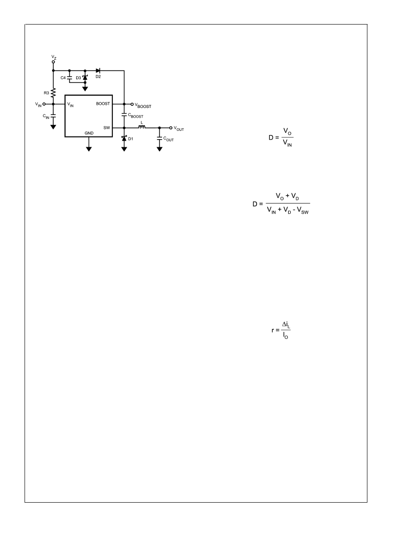
The Duty Cycle (D) can be approximated quickly using the
ratio of output voltage (V
O
) to input voltage (V
IN
):
The catch diode (D1) forward voltage drop and the voltage
drop across the internal NMOS must be included to calculate
a more accurate duty cycle. Calculate D by using the follow-
ing formula:
V
SW
can be approximated by:
V
SW
= I
O
x R
DS(ON)
The diode forward drop (V
) can range from 0.3V to 0.7V
depending on the quality of the diode. The lower V
D
is, the
higher the operating efficiency of the converter.
The inductor value determines the output ripple current.
Lower inductor values decrease the size of the inductor, but
increase the output ripple current.An increase in the inductor
value will decrease the output ripple current. The ratio of
ripple current (
i
) to output current (I
) is optimized when it
is set between 0.3 and 0.4 at 750mA. The ratio r is defined
as:
One must also ensure that the minimum current limit (1.0A)
is not exceeded, so the peak current in the inductor must be
calculated. The peak current (I
LPK
) in the inductor is calcu-
lated by:
I
LPK
= I
O
+
I
L
/2
If r = 0.7 at an output of 750mA, the peak current in the
inductor will be 1.0125A. The minimum guaranteed current
limit over all operating conditions is 1.0A. One can either
reduce r to 0.6 resulting in a 975mA peak current, or make
the engineering judgement that 12.5mA over will be safe
enough with a 1.5A typical current limit and 6 sigma limits.
When the designed maximum output current is reduced, the
ratio r can be increased. At a current of 0.1A, r can be made
as high as 0.9. The ripple ratio can be increased at lighter
loads because the net ripple is actually quite low, and if r
remains constant the inductor value can be made quite
large. An equation empirically developed for the maximum
ripple ratio at any current below 2A is:
r = 0.387 x I
OUT-0.3667
Note that this is just a guideline.
20124248
FIGURE 5. Boost Voltage Supplied from the Shunt
Zener on V
IN
L
www.national.com
9
相關PDF資料 |
PDF描述 |
|---|---|
| LM2736YMKX | Thin SOT23 750mA Load Step-Down DC-DC Regulator |
| LM2750LDX-5.0 | Low Noise, 5.0V Regulated Switched Capacitor Voltage Converter |
| LM2750LD-ADJ | Low Noise, 5.0V Regulated Switched Capacitor Voltage Converter |
| LM2750LDX-ADJ | Low Noise, 5.0V Regulated Switched Capacitor Voltage Converter |
| LM2750LD-5.0 | Low Noise, 5.0V Regulated Switched Capacitor Voltage Converter |
相關代理商/技術參數 |
參數描述 |
|---|---|
| LM2736YMK/NOPB | 功能描述:直流/直流開關調節(jié)器 750MA LOAD STEP-DOWN DC-DC REG RoHS:否 制造商:International Rectifier 最大輸入電壓:21 V 開關頻率:1.5 MHz 輸出電壓:0.5 V to 0.86 V 輸出電流:4 A 輸出端數量: 最大工作溫度: 安裝風格:SMD/SMT 封裝 / 箱體:PQFN 4 x 5 |
| LM2736YMKNOPB | 制造商:National Semiconductor 功能描述:Conv DC-DC Single Step Down 3V to 18V 6-Pin TSOT T/R 制造商:National Semiconductor 功能描述:Conv DC-DC Single Step Down 3V to 18V 6-Pin SOT T/R |
| LM2736YMKX | 功能描述:直流/直流開關調節(jié)器 RoHS:否 制造商:International Rectifier 最大輸入電壓:21 V 開關頻率:1.5 MHz 輸出電壓:0.5 V to 0.86 V 輸出電流:4 A 輸出端數量: 最大工作溫度: 安裝風格:SMD/SMT 封裝 / 箱體:PQFN 4 x 5 |
| LM2736YMKX/NOPB | 功能描述:直流/直流開關調節(jié)器 RoHS:否 制造商:International Rectifier 最大輸入電壓:21 V 開關頻率:1.5 MHz 輸出電壓:0.5 V to 0.86 V 輸出電流:4 A 輸出端數量: 最大工作溫度: 安裝風格:SMD/SMT 封裝 / 箱體:PQFN 4 x 5 |
| LM2737 | 制造商:NSC 制造商全稱:National Semiconductor 功能描述:N-Channel FET Synchronous Buck Regulator Controller for Low Output Voltages |
發(fā)布緊急采購,3分鐘左右您將得到回復。