- 您現(xiàn)在的位置:買賣IC網(wǎng) > PDF目錄385477 > LM2753 (National Semiconductor Corporation) High Power Switched Capacitor Voltage Convertor/Flash LED Driver PDF資料下載
參數(shù)資料
| 型號: | LM2753 |
| 廠商: | National Semiconductor Corporation |
| 元件分類: | LED驅(qū)動(dòng)器 |
| 英文描述: | High Power Switched Capacitor Voltage Convertor/Flash LED Driver |
| 中文描述: | 高功率開關(guān)電容電壓轉(zhuǎn)爐/閃光燈LED驅(qū)動(dòng)器 |
| 文件頁數(shù): | 4/8頁 |
| 文件大小: | 520K |
| 代理商: | LM2753 |
Electrical Characteristics
Note 5:
In applications where high power dissipation and/or poor package thermal resistance is present, the maximum ambient temperature may have to be
derated. Maximum ambient temperature (T
A-MAX
) is dependent on the maximum operationg junction temperature (T
J-MAX-OP
= 120
o
C), the maximum power
dissipation of the device in the application (P
D-MAX
), and the junction-to ambient thermal resistance of the part/package in the application (
θ
JA
), as given by the
following equation: T
A-MAX
= T
J-MAX-OP
- (
θ
JA
x P
D-MAX
).
Note 6:
Junction-to-ambient thermal resistance (
θ
JA
) is taken from a thermal modeling result, performed under the conditions and guidelines set forth in the JEDEC
standard JESD51-7. The test board is a 4 layer FR-4 board measuring 102mm x 76mm x 1.6mm with a 2 x 1 array of thermal vias. The ground plane on the board
is 50mm x 50mm. Thickness of copper layers are 36μm/18μm /18μm/36μm (1.5oz/1oz/1oz/1.5oz). Ambient temperature in simulation is 22C, still air. Power
dissipation is 1W.
The value of
θ
JA
of the LM2753 in LLP-10 could fall in a range as wide as 50
o
C/W to 150
o
C/W (if not wider), depending on PWB material, layout, and environmental
conditions. In applications where high maximum power dissipation exists (high V
, high I
), special care must be paid to thermal dissipation issues. For more
information on these topics, please refer to
Application Note 1187: Leadless Leadframe Package (LLP)
and the
Power Efficiency and Power Dissipation
section of this datasheet..
Note 7:
Min and Max limits are guaranteed by design, test, or statistical analysis. Typical numbers are not guaranteed, but do represent the most likely norm.
Note 8:
C
IN
, C
OUT
, and C
1
: Low-ESR Surface-Mount Ceramic Capacitors (MLCCs) used in setting electrical characteristics
Note 9:
Turn-on time is measured from when the EN signal is pulled high until the output voltage on V
OUT
crosses 90% of its final value.
Note 10:
Flash Turn-on time is measured from when the FLASH signal is pulled high until the voltage on I
OUT
crosses 90% of its final programmed value.
(Notes 2, 7) (Continued)
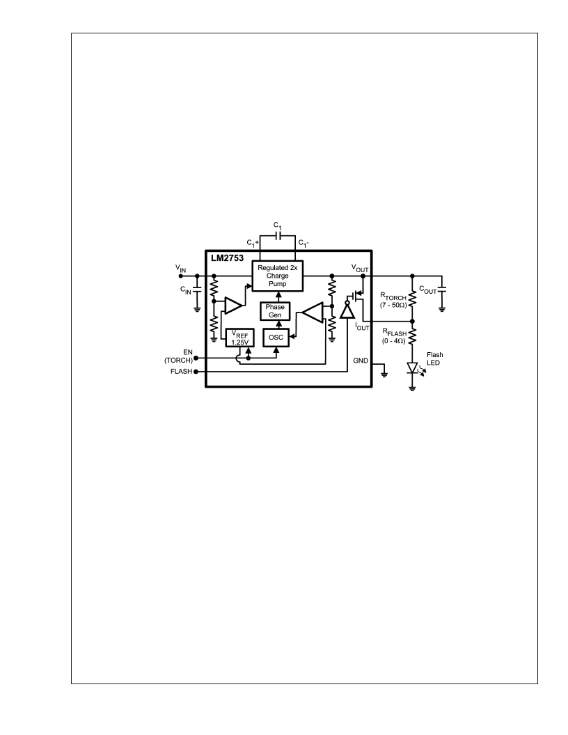
Block Diagram
20140606
L
www.national.com
4
相關(guān)PDF資料 |
PDF描述 |
|---|---|
| LM2753SDX | High Power Switched Capacitor Voltage Convertor/Flash LED Driver |
| LM2765 | Switched Capacitor Voltage Converter |
| LM2765M6 | Switched Capacitor Voltage Converter |
| LM2765M6X | Switched Capacitor Voltage Converter |
| LM2781 | Ultra-Low Ripple Switched Capacitor Voltage Inverter |
相關(guān)代理商/技術(shù)參數(shù) |
參數(shù)描述 |
|---|---|
| LM2753SD | 功能描述:LED照明驅(qū)動(dòng)器 RoHS:否 制造商:STMicroelectronics 輸入電壓:11.5 V to 23 V 工作頻率: 最大電源電流:1.7 mA 輸出電流: 最大工作溫度: 安裝風(fēng)格:SMD/SMT 封裝 / 箱體:SO-16N |
| LM2753SD | 制造商:Texas Instruments 功能描述:VOLT CONV FLASH DRIVER POWERWISE |
| LM2753SD/NOPB | 功能描述:LED照明驅(qū)動(dòng)器 RoHS:否 制造商:STMicroelectronics 輸入電壓:11.5 V to 23 V 工作頻率: 最大電源電流:1.7 mA 輸出電流: 最大工作溫度: 安裝風(fēng)格:SMD/SMT 封裝 / 箱體:SO-16N |
| LM2753SDX | 功能描述:LED照明驅(qū)動(dòng)器 RoHS:否 制造商:STMicroelectronics 輸入電壓:11.5 V to 23 V 工作頻率: 最大電源電流:1.7 mA 輸出電流: 最大工作溫度: 安裝風(fēng)格:SMD/SMT 封裝 / 箱體:SO-16N |
| LM2753SDX/NOPB | 功能描述:LED照明驅(qū)動(dòng)器 RoHS:否 制造商:STMicroelectronics 輸入電壓:11.5 V to 23 V 工作頻率: 最大電源電流:1.7 mA 輸出電流: 最大工作溫度: 安裝風(fēng)格:SMD/SMT 封裝 / 箱體:SO-16N |
發(fā)布緊急采購,3分鐘左右您將得到回復(fù)。