- 您現(xiàn)在的位置:買賣IC網(wǎng) > PDF目錄358837 > LM2991S (NATIONAL SEMICONDUCTOR CORP) Negative Low Dropout Adjustable Regulator PDF資料下載
參數(shù)資料
| 型號: | LM2991S |
| 廠商: | NATIONAL SEMICONDUCTOR CORP |
| 元件分類: | 基準電壓源/電流源 |
| 英文描述: | Negative Low Dropout Adjustable Regulator |
| 中文描述: | 3 V-24 V ADJUSTABLE NEGATIVE LDO REGULATOR, 1 V DROPOUT, PSSO5 |
| 封裝: | PLASTIC, TO-263, 5 PIN |
| 文件頁數(shù): | 3/11頁 |
| 文件大小: | 338K |
| 代理商: | LM2991S |

Absolute Maximum Ratings
(Note 1)
If Military/Aerospace specified devices are required,
please contact the National Semiconductor Sales Office/
Distributors for availability and specifications.
Input Voltage
ESD Susceptibility (Note 2)
Power Dissipation (Note 3)
Junction Temperature (T
Jmax
)
26V to +0.3V
2 kV
Internally limited
125C
Storage Temperature Range
Lead Temperature (Soldering, 10 sec.)
65C to +150C
230C
Operating Ratings
(Note 1)
Junction Temperature Range (T
J
)
Maximum Input Voltage (Operational)
40C to +125C
26V
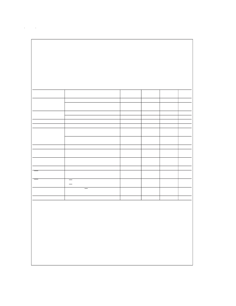
Electrical Characteristics
V
= 10V, V
= 3V, I
= 1A, C
= 47 μF, R1 = 2.7k, T
J
= 25C, unless otherwise specified.
Boldface
limits apply over
the entire operating junction temperature range.
Parameter
Conditions
Typical
(Note 4)
1.210
Min
Max
Units
Reference Voltage
5 mA
≤
I
O
≤
1A
5 mA
≤
I
O
≤
1A,
V
O
1V
≥
V
IN
≥
26V
1.234
1.27
1.186
1.15
V
V
Output Voltage
Range
Line Regulation
Load Regulation
Dropout Voltage
2
25
0.004
0.04
0.1
3
V
V
V
IN
= 26V
I
O
= 5 mA, V
O
1V
≥
V
IN
≥
26V
50 mA
≤
I
O
≤
1A
I
O
= 0.1A,
V
O
≤
100 mV
24
0.04
0.4
0.2
0.3
0.8
1
5
50
%/V
%
V
I
O
= 1A,
V
O
≤
100 mV
0.6
V
Quiescent Current
Dropout Quiescent
Current
Ripple Rejection
I
O
≤
1A
V
IN
= V
O
, I
O
≤
1A
0.7
16
mA
mA
V
ripple
= 1 Vrms, f
ripple
= 1 kHz,
I
O
= 5 mA
10 Hz 100 kHz, I
O
= 5 mA
(V
OUT
: ON)
(V
OUT
: OFF)
V
ON/OFF
= 0.8V (V
OUT
: ON)
V
ON/OFF
= 2.4V (V
OUT
: OFF)
V
IN
= 26V, V
ON/OFF
= 2.4V
V
OUT
= 0V
V
OUT
= 0V
60
50
dB
Output Noise
ON /OFF Input
Voltage
ON /OFF Input
Current
Output Leakage
Current
Current Limit
200
1.2
1.3
0.1
40
60
450
0.8
μV
V
2.4
10
100
250
μA
μA
2
1.5
A
Note 1:
Absolute Maximum Ratings indicate limits beyond which damage to the device may occur. Operating Ratings indicate conditions for which the deivce is in-
tended to be functional, but do not guarantee specific performance limits. For guaranteed specifications and test conditions, see the Electrical Characteristics.
Note 2:
Human body model, 100 pF discharged through a 1.5 k
resistor.
Note 3:
The maximum power dissipation is a function of T
,
θ
and T
. The maximum allowable power dissipation at any ambient temperature is P
= (T
T
)/
θ
. If this dissipation is exceeded, the die temperature will rise above 125C and the LM2991 will go into thermal shutdown. For the LM2991, the
junction-to-ambient thermal resistance is 53C/W for the TO-220, 73C/W for the TO-263, and junction-to-case thermal resistance is 3C. If the TO-263 package is
used, the thermal resistance can be reduced by increasing the PC board copper area thermally connected to the package. Using 0.5 square inches of copper area,
θ
JA
is 50C/W; with 1 square inch of copper area,
θ
JA
is 37C/W; and with 1.6 or more square inches of copper area,
θ
JA
is 32C/W.
Note 4:
Typicals are at T
J
= 25C and represent the most likely parametric norm.
www.national.com
3
相關PDF資料 |
PDF描述 |
|---|---|
| LM2991 | Negative Low Dropout Adjustable Regulator |
| LM3-EWN1-01-N2 | SMD LED |
| LM3-PBG1-01-N1 | SMD LED |
| LM3-PBL1-01-N1 | SMD LED |
| LM3-PPG1-01-N1 | SMD LED |
相關代理商/技術參數(shù) |
參數(shù)描述 |
|---|---|
| LM2991S | 制造商:Texas Instruments 功能描述:V REG ADJ -2/25V 2991 TO-263-5 |
| LM2991S/NOPB | 功能描述:低壓差穩(wěn)壓器 - LDO NEG LDO ADJ REG RoHS:否 制造商:Texas Instruments 最大輸入電壓:36 V 輸出電壓:1.4 V to 20.5 V 回動電壓(最大值):307 mV 輸出電流:1 A 負載調節(jié):0.3 % 輸出端數(shù)量: 輸出類型:Fixed 最大工作溫度:+ 125 C 安裝風格:SMD/SMT 封裝 / 箱體:VQFN-20 |
| LM2991S/NOPB | 制造商:Texas Instruments 功能描述:Linear Voltage Regulator IC |
| LM2991SP | 制造商:NATIONAL 功能描述:NEW 制造商:Texas Instruments 功能描述: |
| LM2991SX | 功能描述:低壓差穩(wěn)壓器 - LDO RoHS:否 制造商:Texas Instruments 最大輸入電壓:36 V 輸出電壓:1.4 V to 20.5 V 回動電壓(最大值):307 mV 輸出電流:1 A 負載調節(jié):0.3 % 輸出端數(shù)量: 輸出類型:Fixed 最大工作溫度:+ 125 C 安裝風格:SMD/SMT 封裝 / 箱體:VQFN-20 |
發(fā)布緊急采購,3分鐘左右您將得到回復。