- 您現(xiàn)在的位置:買賣IC網(wǎng) > PDF目錄358837 > LM3046N (NATIONAL SEMICONDUCTOR CORP) LM3045/LM3046/LM3086 Transistor Arrays PDF資料下載
參數(shù)資料
| 型號: | LM3046N |
| 廠商: | NATIONAL SEMICONDUCTOR CORP |
| 元件分類: | 小信號晶體管 |
| 英文描述: | LM3045/LM3046/LM3086 Transistor Arrays |
| 中文描述: | 5 CHANNEL, VHF BAND, Si, NPN, RF SMALL SIGNAL TRANSISTOR |
| 文件頁數(shù): | 3/6頁 |
| 文件大小: | 197K |
| 代理商: | LM3046N |

Electrical Characteristics
(Continued)
(T
A
= 25C unless otherwise specified)
Parameter
Conditions
Limits
Typ
1.1
Units
Min
Max
Temperature Coefficient of
Input Offset Voltage
V
CE
= 3V, I
C
= 1 mA
μV/C
Note 1:
“Absolute Maximum Ratings” indicate limits beyond which damage to the device may occur. Operating Ratings indicate conditions for which the device is
functional, but do not guarantee specific performance limits.
Note 2:
The collector of each transistor is isolated from the substrate by an integral diode. The substrate (terminal 13) must be connected to the most negative point
in the external circuit to maintain isolation between transistors and to provide for normal transistor action.
Electrical Characteristics
Parameter
Conditions
Min
Typ
3.25
Max
Units
dB
Low Frequency Noise Figure (NF)
f = 1 kHz, V
CE
= 3V,
I
C
= 100 μA, R
S
= 1 k
LOW FREQUENCY, SMALL SIGNAL EQUIVALENT CIRCUIT CHARACTERISTICS
Forward Current Transfer Ratio (h
fe
)
f = 1 kHz, V
CE
= 3V,
I
C
= 1 mA
110
Short Circuit Input Impednace (h
ie
)
Open Circuit Output Impedance (h
oe
)
Open Circuit Reverse Voltage Transfer Ratio
(h
re
)
ADMITTANCE CHARACTERISTICS
Forward Transfer Admittance (Y
fe
)
Input Admittance (Y
ie
)
Output Admittance (Y
oe
)
Reverse Transfer Admittance (Y
re
)
Gain Bandwidth Product (f
T
)
Emitter to Base Capacitance (C
EB
)
Collector to Base Capacitance (C
CB
)
Collector to Substrate Capacitance (C
CI
)
3.5
15.6
k
μmho
1.8 x 10
4
f = 1 MHz, V
CE
= 3V,
I
C
= 1 mA
31 j 1.5
0.3+J 0.04
0.001+j 0.03
See Curve
550
0.6
0.58
2.8
V
CE
= 3V, I
C
= 3 mA
V
EB
= 3V, I
E
= 0
V
CB
= 3V, I
C
= 0
V
CS
= 3V, I
C
= 0
300
pF
pF
pF
Typical Performance Characteristics
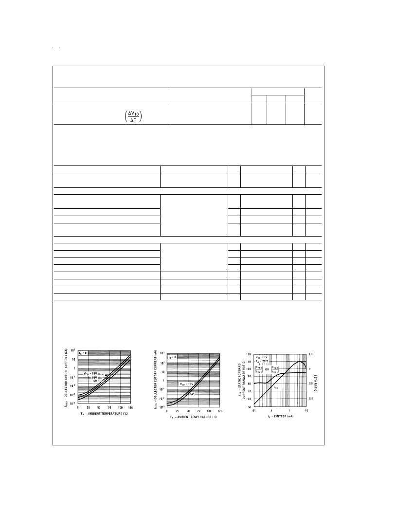
Typical Collector To Base
Cutoff Current vs Ambient
Temperature for Each
Transistor
DS007950-8
Typical Collector To Emitter
Cutoff Current vs Ambient
Temperature for Each
Transistor
DS007950-9
Typical Static Forward
Current-Transfer Ratio and
Beta Ratio for Transistors Q
1
and Q
2
vs Emitter Current
DS007950-10
www.national.com
3
相關(guān)PDF資料 |
PDF描述 |
|---|---|
| LM3046M | LM3045/LM3046/LM3086 Transistor Arrays |
| LM305A | Voltage Regulators |
| LM305H | Voltage Regulators |
| LM305AH | CAP 10V 1000UF SOLID ELECT AXIAL |
| LM305 | Voltage Regulators |
相關(guān)代理商/技術(shù)參數(shù) |
參數(shù)描述 |
|---|---|
| LM304H | 制造商:Texas Instruments 功能描述: |
| LM304H/A+ | 制造商:未知廠家 制造商全稱:未知廠家 功能描述:Negative Adjustable Voltage Regulator |
| LM305 | 制造商:INTERSIL 制造商全稱:Intersil Corporation 功能描述:N-CHANNEL JFET |
| LM3053H | 制造商:Texas Instruments 功能描述: |
| LM305A | 制造商:NSC 制造商全稱:National Semiconductor 功能描述:Voltage Regulators |
發(fā)布緊急采購,3分鐘左右您將得到回復(fù)。