- 您現(xiàn)在的位置:買賣IC網(wǎng) > PDF目錄358843 > LM340AT-06 (Motorola, Inc.) THREE-TERMINAL POSITIVE FIXED VOLTAGE REGULATORS PDF資料下載
參數(shù)資料
| 型號(hào): | LM340AT-06 |
| 廠商: | Motorola, Inc. |
| 元件分類: | 基準(zhǔn)電壓源/電流源 |
| 英文描述: | THREE-TERMINAL POSITIVE FIXED VOLTAGE REGULATORS |
| 中文描述: | 三端固定電壓調(diào)節(jié)器 |
| 文件頁(yè)數(shù): | 3/20頁(yè) |
| 文件大小: | 205K |
| 代理商: | LM340AT-06 |
第1頁(yè)第2頁(yè)當(dāng)前第3頁(yè)第4頁(yè)第5頁(yè)第6頁(yè)第7頁(yè)第8頁(yè)第9頁(yè)第10頁(yè)第11頁(yè)第12頁(yè)第13頁(yè)第14頁(yè)第15頁(yè)第16頁(yè)第17頁(yè)第18頁(yè)第19頁(yè)第20頁(yè)

LM340, A Series
3
MOTOROLA ANALOG IC DEVICE DATA
LM340–5.0
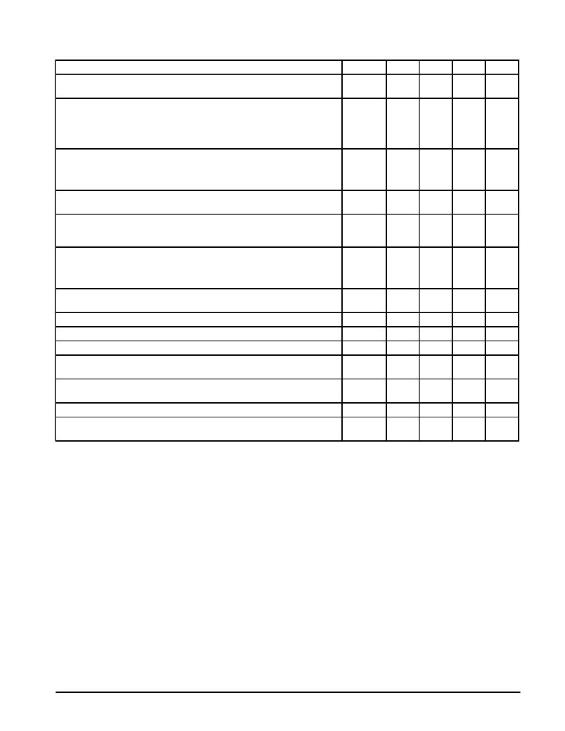
ELECTRICAL CHARACTERISTICS
(Vin = 10 V, IO = 500 mA, TJ = Tlow to Thigh [Note 1], unless otherwise noted.)
Characteristics
Symbol
Min
Typ
Max
Unit
Output Voltage (TJ = +25
°
C)
IO = 5.0 mA to 1.0 A
VO
4.8
5.0
5.2
Vdc
Line Regulation (Note 2)
8.0 Vdc to 20 Vdc
7.0 Vdc to 25 Vdc (TJ = +25
°
C)
8.0 Vdc to 12 Vdc, IO = 1.0 A
7.3 Vdc to 20 Vdc, IO = 1.0 A (TJ = +25
°
C)
Load Regulation (Note 2)
5.0 mA
≤
IO
≤
1.0 A
5.0 mA
≤
IO
≤
1.5 A (TJ = +25
°
C)
250 mA
≤
IO
≤
750 mA (TJ = +25
°
C)
Regline
–
–
–
–
–
–
–
–
50
50
25
50
mV
Regload
–
–
–
–
–
–
50
50
25
mV
Output Voltage
7.0
≤
Vin
≤
20 Vdc, 5.0 mA
≤
IO
≤
1.0 A, PD
≤
15 W
VO
4.75
–
5.25
Vdc
Quiescent Current
IO = 1.0 A
TJ = +25
°
C
IB
–
–
–
4.0
8.5
8.0
mA
Quiescent Current Change
7.0
≤
Vin
≤
25 Vdc, IO = 500 mA
5.0 mA
≤
IO
≤
1.0 A, Vin = 10 V
7.5
≤
Vin
≤
20 Vdc, IO = 1.0 A
IB
–
–
–
–
–
–
1.0
0.5
1.0
mA
Ripple Rejection
IO = 1.0 A (TJ = +25
°
C)
RR
62
80
–
dB
Dropout Voltage
VI – VO
rO
ISC
Vn
–
1.7
–
Vdc
Output Resistance (f = 1.0 kHz)
–
2.0
–
m
Short Circuit Current Limit (TJ = +25
°
C)
Output Noise Voltage (TA = +25
°
C)
10 Hz
≤
f
≤
100 kHz
–
2.0
–
A
–
40
–
μ
V
Average Temperature Coefficient of Output Voltage
IO = 5.0 mA
TCVO
–
±
0.6
–
mV/
°
C
Peak Output Current (TJ = +25
°
C)
Input Voltage to Maintain Line Regulation (TJ = +25
°
C)
IO = 1.0 A
IO
–
2.4
–
A
7.3
–
–
Vdc
NOTES:
1.Tlow to Thigh = 0
°
to +125
°
C
2.Load and line regulation are specified at constant junction temperature. Changes in VO due to heating effects must be taken into account separately.
Pulse testing with low duty cycle is used.
DEFINITIONS
Line Regulation
– The change in output voltage for a
change in the input voltage. The measurement is made
under conditions of low dissipation or by using pulse
techniques such that the average chip temperature is not
significantly affected.
Load Regulation
– The change in output voltage for a
change in load current at constant chip temperature.
Maximum Power Dissipation
– The maximum total device
dissipation for which the regulator will operate within
specifications.
Quiescent Current
– That part of the input current that is not
delivered to the load.
Output Noise Voltage
– The rms AC voltage at the output,
with constant load and no input ripple, measured over a
specified frequency range.
相關(guān)PDF資料 |
PDF描述 |
|---|---|
| LM340AT-08 | THREE-TERMINAL POSITIVE FIXED VOLTAGE REGULATORS |
| LM340AT-09 | THREE-TERMINAL POSITIVE FIXED VOLTAGE REGULATORS |
| LM340AT-18 | THREE-TERMINAL POSITIVE FIXED VOLTAGE REGULATORS |
| LM340AT-24 | THREE-TERMINAL POSITIVE FIXED VOLTAGE REGULATORS |
| LM340T-05 | THREE-TERMINAL POSITIVE FIXED VOLTAGE REGULATORS |
相關(guān)代理商/技術(shù)參數(shù) |
參數(shù)描述 |
|---|---|
| LM340AT-08 | 制造商:MOTOROLA 制造商全稱:Motorola, Inc 功能描述:THREE TERMINAL POSITIVE FIXED VOLTAGE REGULATORS |
| LM340AT-09 | 制造商:MOTOROLA 制造商全稱:Motorola, Inc 功能描述:THREE TERMINAL POSITIVE FIXED VOLTAGE REGULATORS |
| LM340AT-12 | 制造商:MOTOROLA 制造商全稱:Motorola, Inc 功能描述:THREE TERMINAL POSITIVE FIXED VOLTAGE REGULATORS |
| LM340AT-15 | 制造商:OC White Company 功能描述:LDO Regulator Pos 15V 1A 3-Pin(3+Tab) TO-220 Rail |
| LM340AT-18 | 制造商:MOTOROLA 制造商全稱:Motorola, Inc 功能描述:THREE TERMINAL POSITIVE FIXED VOLTAGE REGULATORS |
發(fā)布緊急采購(gòu),3分鐘左右您將得到回復(fù)。