- 您現(xiàn)在的位置:買賣IC網(wǎng) > PDF目錄39248 > LM3460M5X-1.5/NOPB (NATIONAL SEMICONDUCTOR CORP) 1-OUTPUT THREE TERM VOLTAGE REFERENCE, 1.5 V, PDSO5 PDF資料下載
參數(shù)資料
| 型號(hào): | LM3460M5X-1.5/NOPB |
| 廠商: | NATIONAL SEMICONDUCTOR CORP |
| 元件分類: | 基準(zhǔn)電壓源/電流源 |
| 英文描述: | 1-OUTPUT THREE TERM VOLTAGE REFERENCE, 1.5 V, PDSO5 |
| 封裝: | SOT-23, 5 PIN |
| 文件頁數(shù): | 6/9頁 |
| 文件大小: | 582K |
| 代理商: | LM3460M5X-1.5/NOPB |
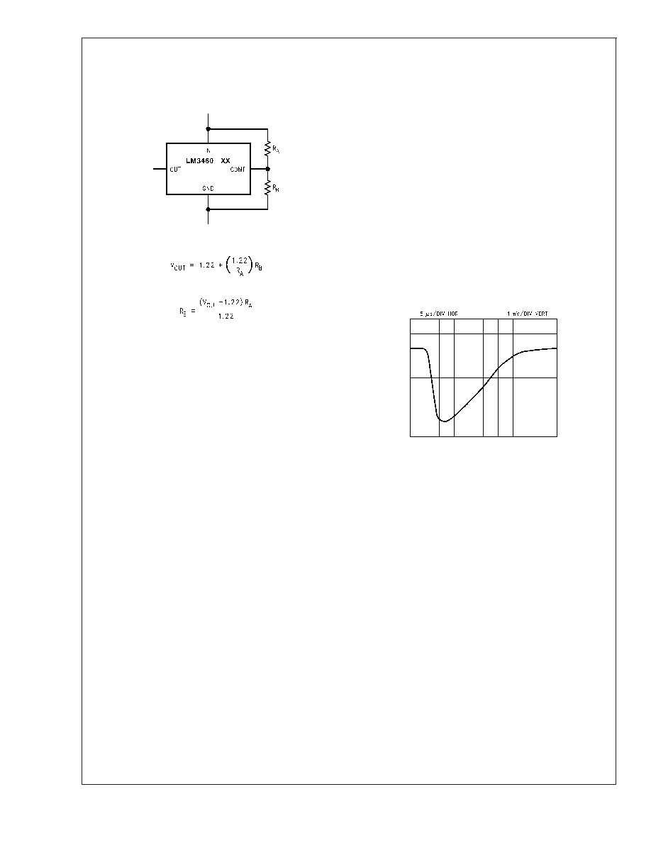
Setting the Output Voltage
If a regulated voltage is desired which is not available as a
standard voltage, the output voltage may be adjusted by
using an external resistive divider (see Figure 4):
The simplest way to calculate the resistor values is to as-
sume a value for R
A and then solve the equation shown for
R
B.
To assure best output voltage accuracy, the value selected
for R
A should be < 500
, and 1% tolerance resistors should
be used.
As the ohmic value of R
A is increased, the internal resistive
divider inside the LM3460 will cause the output voltage to
deviate from the value predicted by the formula shown.
App Circuit Technical Information
LM3460. This section provides details of circuit function.
1.5V/7A TYPICAL APPLICATION
Figure 1 shows the schematic of a wide-bandwidth linear
regulator which provides a regulated 1.5V output at up to 7A
of load current from a 3V-3.6V input.
The pass element of the regulator (which supplies the load
current) is made up of a three-transistor complimentary Dar-
lington composed of Q2, Q3, and Q4. The bias current
flowing through R1 will drive the pass element ON, until such
time as Q1 pulls down and takes the drive away from the
base of Q2.
The circuit regulates the output to 1.5V using the LM3460
precision controller, which sources current from its output
whenever the voltage at the IN pin reaches 1.5V.
When the LM3460 sources current from its output, it turns on
Q1 (stealing the base drive for Q2) which reduces the cur-
rent from the 1.5V regulated output. In this way, a negative
feedback loop is established which locks the output at 1.5V.
C1 and C2 are used for compensation, and should be ce-
ramic capacitors.
C4 is required for regulator stability, and both C3 and C4
affect transient response. Circuit performance should be
carefully evaluated if substitutions are made for these two
components.
PERFORMANCE DATA
All data taken at 20C ambient:
LOAD/LINE REGULATION: The output voltage changed
<0.1 mV as the load was increased from 0-7A, and the input
voltage was varied from 3.0V-3.6V.
DROPOUT VOLTAGE: The dropout voltage (which is de-
fined as the minimum input-output voltage differential re-
quired to maintain a regulated output) was measured at 7A
and found to be 1.4V. This means that a minimum input
voltage of 2.9V is required to keep the 1.5V output in regu-
lation.
TRANSIENT RESPONSE: Transient response was tested
using a 0.2
power resistor connected to the output using a
mechanical contact to provide a 0-7A load current step.
When the load was applied, the change in output voltage
was seen to be < 5 mV with a total recovery time of about 30
s (see Figure 5).
HEATSINKING/COMPONENT SELECTION
HEATSINKING: As with any linear regulator, the power dis-
sipated in the pass transistor (Q4) is approximately:
P= (V
INVOUT)XILOAD
Q4 must be provided with adequate heatsinking so that the
junction temperature never exceeds 150C.
Figure 6 shows the maximum allowable values of thermal
resistance (from heatsink-to-ambient) that must be provided
for various values of the load current.
01260310
FOR BEST RESULTS: SELECT R
A < 500
FIGURE 4. Setting the Output Voltage
01260311
FIGURE 5. Output Transient Response
LM3460
www.national.com
6
相關(guān)PDF資料 |
PDF描述 |
|---|---|
| LM3670MFX-2.5/NOPB | 0.75 A SWITCHING REGULATOR, 1300 kHz SWITCHING FREQ-MAX, PDSO5 |
| LM368H-6.2 | 1-OUTPUT TWO TERM VOLTAGE REFERENCE, 6.2 V, MBCY8 |
| LM368YH-6.2 | 1-OUTPUT TWO TERM VOLTAGE REFERENCE, 6.2 V, MBCY8 |
| LM385AXM-2.5X | 1-OUTPUT TWO TERM VOLTAGE REFERENCE, 2.5 V, PDSO8 |
| LM285AM-2.5X | 1-OUTPUT TWO TERM VOLTAGE REFERENCE, 2.5 V, PDSO8 |
相關(guān)代理商/技術(shù)參數(shù) |
參數(shù)描述 |
|---|---|
| LM3463 | 制造商:TI 制造商全稱:Texas Instruments 功能描述:Dynamic Headroom Controller with Thermal Control Interface and Individual Channel Dimming Control |
| LM3463_12 | 制造商:TI 制造商全稱:Texas Instruments 功能描述:LM3463 Dynamic Headroom Controller with Thermal Control Interface and Individual Channel Dimming Control |
| LM3463EVM | 功能描述:LED 照明開發(fā)工具 LM3463EVM Eval Mod RoHS:否 制造商:Fairchild Semiconductor 產(chǎn)品:Evaluation Kits 用于:FL7732 核心: 電源電壓:120V 系列: 封裝: |
| LM3463EVM | 制造商:Texas Instruments 功能描述:EVAL BOARD, LM3463 200mA LED DRIVER |
| LM3463SQ | 制造商:TI 制造商全稱:Texas Instruments 功能描述:Dynamic Headroom Controller with Thermal Control Interface and Individual Channel Dimming Control |
發(fā)布緊急采購(gòu),3分鐘左右您將得到回復(fù)。