- 您現(xiàn)在的位置:買賣IC網(wǎng) > PDF目錄30750 > LM3876MDC (NATIONAL SEMICONDUCTOR CORP) 56 W, 1 CHANNEL, AUDIO AMPLIFIER, UUC PDF資料下載
參數(shù)資料
| 型號(hào): | LM3876MDC |
| 廠商: | NATIONAL SEMICONDUCTOR CORP |
| 元件分類: | 音頻/視頻放大 |
| 英文描述: | 56 W, 1 CHANNEL, AUDIO AMPLIFIER, UUC |
| 封裝: | DIE |
| 文件頁數(shù): | 17/22頁 |
| 文件大小: | 613K |
| 代理商: | LM3876MDC |

Electrical Characteristics (Notes 4, 5) (Continued)
The following specifications apply for V
+ = +35V, V = 35V, I
MUTE = 0.5 mA with RL =8 unless otherwise specified. Limits
apply for T
A = 25C.
Symbol
Parameter
Conditions
LM3876
Units
(Limits)
Typical
Limit
(Note 9) (Note 10)
e
IN
(Note 3)
Input Noise
IHF — A Weighting Filter
2.0
8
V (max)
R
IN = 600 (Input Referred)
SNR
Signal-to-Noise Ratio
P
O = 1W, A-Weighted,
98
dB
Measured at 1 kHz, R
S =25
P
O = 40W, A-Weighted,
114
dB
Measured at 1 kHz, R
S =25
Ppk= 100W, A-Weighted,
122
dB
Measured at 1 kHz, R
S =25
IMD
Intermodulation Distortion Test
60 Hz, 7 kHz, 4:1 (SMPTE)
0.004
%
60 Hz, 7 kHz, 1:1 (SMPTE)
0.006
Note 2: DC Electrical Test; refer to Test Circuit #1.
Note 3: AC Electrical Test; refer to Test Circuit #2.
Note 4: All voltages are measured with respect to the GND pin (pin 7), unless otherwise specified.
Note 5: Absolute Maximum Ratings indicate limits beyond which damage to the device may occur. Operating Ratings indicate conditions for which the device is
functional, but do not guarantee specific performance limits. Electrical Characteristics state DC and AC electrical specifications under particular test conditions which
guarantee specific performance limits. This assumes that the device is within the Operating Ratings. Specifications are not guaranteed for parameters where no limit
is given, however, the typical value is a good indication of device performance.
Note 6: For operating at case temperatures above 25C, the device must be derated based on a 150C maximum junction temperature and a thermal resistance of
θJC = 1.0 C/W (junction to case). Refer to the Thermal Resistance figure in the Application Information section under Thermal Considerations.
Note 7: Human body model, 100 pF discharged through a 1.5 k
resistor.
Note 8: The operating junction temperature maximum is 150C, however, the instantaneous Safe Operating Area temperature is 250C.
Note 9: Typicals are measured at 25C and represent the parametric norm.
Note 10: Limits are guaranteed to National’s AOQL (Average Outgoing Quality Level).
Note 11: The LM3876T package TA11B is a non-isolated package, setting the tab of the device and the heat sink at V potential when the LM3876 is directly
mounted to the heat sink using only thermal compound. If a mica washer is used in addition to thermal compound,
θCS (case to sink) is increased, but the heat sink
will be isolated from V.
Note 12: The feedback compensation network limits the bandwidth of the closed-loop response and so the slew rate will be reduced due to the high frequency
roll-off. Without feedback compensation, the slew rate is typically 16V/s.
Note 13: V must have at least 9V at its pin with reference to ground in order for the under-voltage protection circuitry to be disabled.
Note 14: The output dropout voltage is the supply voltage minus the clipping voltage. Refer to the Clipping Voltage vs Supply Voltage graph in the Typical Perfor-
mance Characteristics section.
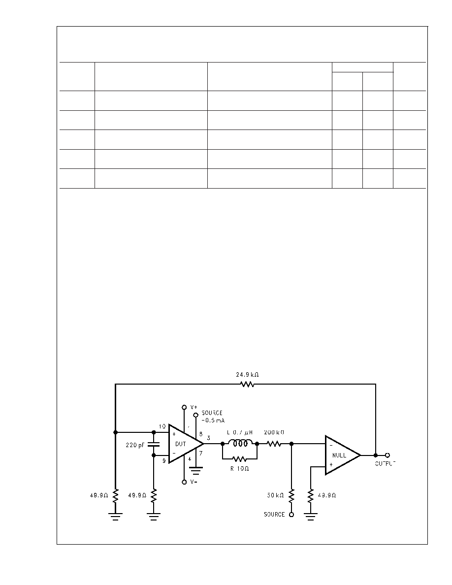
Test Circuit #1 (DC Electrical Test Circuit)
DS011832-3
LM3876
www.national.com
4
相關(guān)PDF資料 |
PDF描述 |
|---|---|
| LM387N | VIDEO PREAMPLIFIER, PDIP8 |
| LM387V | 2 CHANNEL, VIDEO PREAMPLIFIER, PDIP8 |
| LM3886DWF | 68 W, 1 CHANNEL, AUDIO AMPLIFIER, UUC |
| LM3886MWC | 68 W, 1 CHANNEL, AUDIO AMPLIFIER, UUC |
| LM3909N | SPECIALTY CONSUMER CIRCUIT, PDIP8 |
相關(guān)代理商/技術(shù)參數(shù) |
參數(shù)描述 |
|---|---|
| LM3876T | 功能描述:音頻放大器 RoHS:否 制造商:STMicroelectronics 產(chǎn)品:General Purpose Audio Amplifiers 輸出類型:Digital 輸出功率: THD + 噪聲: 工作電源電壓:3.3 V 電源電流: 最大功率耗散: 最大工作溫度: 安裝風(fēng)格:SMD/SMT 封裝 / 箱體:TQFP-64 封裝:Reel |
| LM3876T | 制造商:National Semiconductor Corporation 功能描述:56W W/Mute, 1 Channel Lm3876T IC Audio Amp |
| LM3876T/NOPB | 功能描述:音頻放大器 RoHS:否 制造商:STMicroelectronics 產(chǎn)品:General Purpose Audio Amplifiers 輸出類型:Digital 輸出功率: THD + 噪聲: 工作電源電壓:3.3 V 電源電流: 最大功率耗散: 最大工作溫度: 安裝風(fēng)格:SMD/SMT 封裝 / 箱體:TQFP-64 封裝:Reel |
| LM3876TF | 功能描述:音頻放大器 RoHS:否 制造商:STMicroelectronics 產(chǎn)品:General Purpose Audio Amplifiers 輸出類型:Digital 輸出功率: THD + 噪聲: 工作電源電壓:3.3 V 電源電流: 最大功率耗散: 最大工作溫度: 安裝風(fēng)格:SMD/SMT 封裝 / 箱體:TQFP-64 封裝:Reel |
| LM3876TF NOPB | 制造商:Texas Instruments 功能描述:8MHz Class-AB Bulk |
發(fā)布緊急采購,3分鐘左右您將得到回復(fù)。