- 您現(xiàn)在的位置:買賣IC網(wǎng) > PDF目錄358860 > LM4041AIM3-1.2 (NATIONAL SEMICONDUCTOR CORP) Precision Micropower Shunt Voltage Reference PDF資料下載
參數(shù)資料
| 型號(hào): | LM4041AIM3-1.2 |
| 廠商: | NATIONAL SEMICONDUCTOR CORP |
| 元件分類: | 基準(zhǔn)電壓源/電流源 |
| 英文描述: | Precision Micropower Shunt Voltage Reference |
| 中文描述: | 1-OUTPUT TWO TERM VOLTAGE REFERENCE, 1.225 V, PDSO3 |
| 封裝: | PLASTIC, TO-236AB, SOT-23, 3 PIN |
| 文件頁(yè)數(shù): | 8/19頁(yè) |
| 文件大小: | 343K |
| 代理商: | LM4041AIM3-1.2 |
第1頁(yè)第2頁(yè)第3頁(yè)第4頁(yè)第5頁(yè)第6頁(yè)第7頁(yè)當(dāng)前第8頁(yè)第9頁(yè)第10頁(yè)第11頁(yè)第12頁(yè)第13頁(yè)第14頁(yè)第15頁(yè)第16頁(yè)第17頁(yè)第18頁(yè)第19頁(yè)

Electrical Characteristics (continued)
Note 1:
Absolute Maximum Ratings indicate limits beyond which damage to the device may occur. Operating Ratings indicate conditions for which the device is
functional, but do not guarantee specific performance limits. For guaranteed specifications and test conditions, see the Electrical Characteristics. The guaranteed
specifications apply only for the test conditions listed. Some performance characteristics may degrade when the device is not operated under the listed test
conditions.
Note 2:
The maximum power dissipation must be derated at elevated temperatures and is dictated by T
Jmax
(maximum junction temperature),
θ
JA
(junction to
ambient thermal resistance), and T
A
(ambient temperature). The maximum allowable power dissipation at any temperature is PD
max
= (T
Jmax
T
A
)/
θ
JA
or the
number given in the Absolute Maximum Ratings, whichever is lower. For the LM4041, T
Jmax
= 125C, and the typical thermal resistance (
θ
JA
), when board mounted,
is 326C/W for the SOT-23 package, 415C/W for the SC70 package and 180C/W with 0.4" lead length and 170C/W with 0.125" lead length for the TO-92 package.
Note 3:
The human body model is a 100 pF capacitor discharged through a 1.5 k
resistor into each pin. The machine model is a 200 pF capacitor discharged
directly into each pin. All pins are rated at 2kV for Human Body Model, but the feedback pin which is rated at 1kV.
Note 4:
Typicals are at T
J
= 25C and represent most likely parametric norm.
Note 5:
Limits are 100% production tested at 25C. Limits over temperature are guaranteed through correlation using Statistical Quality Control (SQC) methods.
The limits are used to calculate National’s AOQL.
Note 6:
The boldface (over-temperature) limit for Reverse Breakdown Voltage Tolerance is defined as the room temperature Reverse Breakdown Voltage Tolerance
±
[(
V
R
v
T)(max
T)(V
R
)]. Where,
V
/
T is the V
temperature coefficient, max
T is the maximum difference in temperature from the reference point of 25 C
to T
MAX
or T
MIN
, and V
R
is the reverse breakdown voltage. The total over-temperature tolerance for the different grades in the industrial temperature range where
max
A-grade:
±
0.75% =
±
0.1%
±
100 ppm/C x 65C
B-grade:
±
0.85% =
±
0.2%
±
100 ppm/C x 65C
C-grade:
±
1.15% =
±
0.5%
±
100 ppm/C x 65C
D-grade:
±
1.98% =
±
1.0%
±
150 ppm/C x 65C
E-grade:
±
2.98% =
±
2.0%
±
150 ppm/C x 65C
The total over-temperature tolerance for the different grades in the extended temperature range where max
T = 100 C is shown below:
B-grade:
±
1.2% =
±
0.2%
±
100 ppm/C x 100C
C-grade:
±
1.5% =
±
0.5%
±
100 ppm/C x 100C
D-grade:
±
2.5% =
±
1.0%
±
150 ppm/C x 100C
E-grade:
±
4.5% =
±
2.0%
±
150 ppm/C x 100C
Therefore, as an example, the A-grade LM4041-1.2 has an over-temperature Reverse Breakdown Voltage tolerance of
±
1.2V x 0.75% =
±
9.2 mV.
Note 7:
When V
≤
1.6V, the LM4041-ADJ in the SOT-23 package must operate at reduced I
. This is caused by the series resistance of the die attach between
the die (-) output and the package (-) output pin. See the Output Saturation (SOT-23 only) curve in the Typical Performance Characteristics section.
Note 8:
Reference voltage and temperature coefficient will change with output voltage. See Typical Performance Characteristics curves.
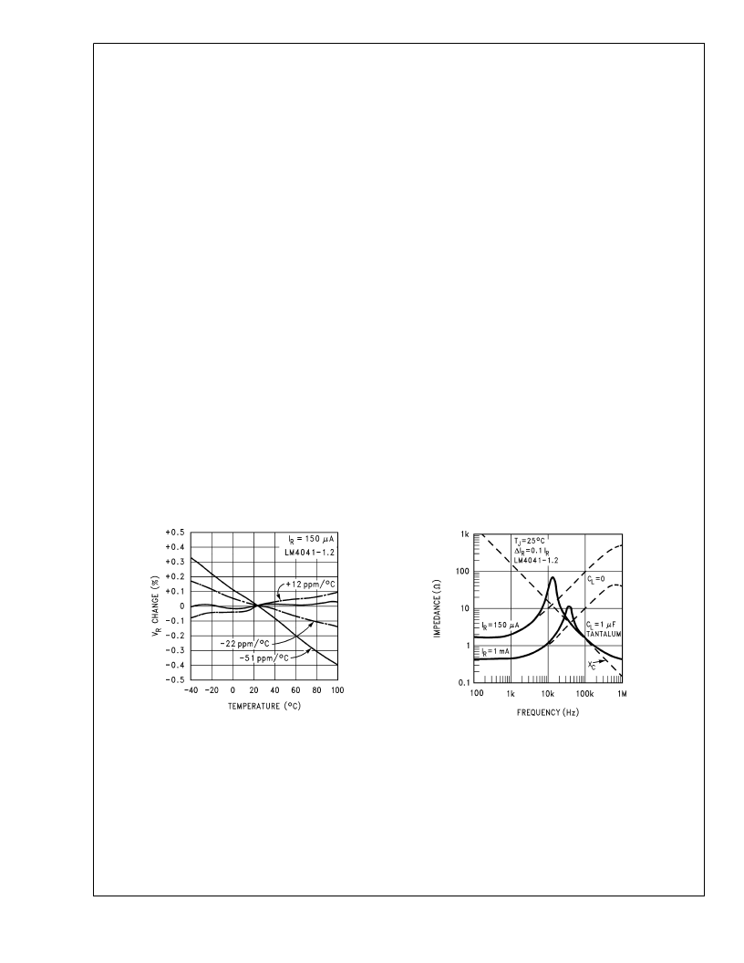
Typical Performance Characteristics
Temperature Drift for Different
Average Temperature Coefficient
DS011392-19
Output Impedance vs Frequency
DS011392-4
L
www.national.com
8
相關(guān)PDF資料 |
PDF描述 |
|---|---|
| LM4041AIM3-1.2 | Precision Micropower Shunt Voltage Reference |
| LM4050AEM3-2.1-T | 50ppm/∑C Precision Micropower Shunt Voltage References with Multiple Reverse Breakdown Voltages |
| LM4050AIM3-10 | Precision Micropower Shunt Voltage Reference |
| LM4050BIM3X-2.5 | Precision Micropower Shunt Voltage Reference |
| LM4050CIM3X-2.5 | KK 156 PCB Assy RtAn 09 Ckt Tin RoHS Compliant: Yes |
相關(guān)代理商/技術(shù)參數(shù) |
參數(shù)描述 |
|---|---|
| LM4041AIM3-4.1 | 制造商:Maxim Integrated Products 功能描述:- Rail/Tube |
| LM4041AIM3X-1.2 | 功能描述:基準(zhǔn)電壓& 基準(zhǔn)電流 RoHS:否 制造商:STMicroelectronics 產(chǎn)品:Voltage References 拓?fù)浣Y(jié)構(gòu):Shunt References 參考類型:Programmable 輸出電壓:1.24 V to 18 V 初始準(zhǔn)確度:0.25 % 平均溫度系數(shù)(典型值):100 PPM / C 串聯(lián) VREF - 輸入電壓(最大值): 串聯(lián) VREF - 輸入電壓(最小值): 分流電流(最大值):60 mA 最大工作溫度:+ 125 C 封裝 / 箱體:SOT-23-3L 封裝:Reel |
| LM4041AIM3X-1.2/NOPB | 功能描述:基準(zhǔn)電壓& 基準(zhǔn)電流 RoHS:否 制造商:STMicroelectronics 產(chǎn)品:Voltage References 拓?fù)浣Y(jié)構(gòu):Shunt References 參考類型:Programmable 輸出電壓:1.24 V to 18 V 初始準(zhǔn)確度:0.25 % 平均溫度系數(shù)(典型值):100 PPM / C 串聯(lián) VREF - 輸入電壓(最大值): 串聯(lián) VREF - 輸入電壓(最小值): 分流電流(最大值):60 mA 最大工作溫度:+ 125 C 封裝 / 箱體:SOT-23-3L 封裝:Reel |
| LM4041AIM3X12 | 制造商:NATIONAL 功能描述:* |
| LM4041AIM3X41 | 制造商:NATIONAL 功能描述:* |
發(fā)布緊急采購(gòu),3分鐘左右您將得到回復(fù)。