- 您現(xiàn)在的位置:買賣IC網(wǎng) > PDF目錄30751 > LM4546AVH/NOPB (NATIONAL SEMICONDUCTOR CORP) SPECIALTY CONSUMER CIRCUIT, PQFP48 PDF資料下載
參數(shù)資料
| 型號: | LM4546AVH/NOPB |
| 廠商: | NATIONAL SEMICONDUCTOR CORP |
| 元件分類: | 消費家電 |
| 英文描述: | SPECIALTY CONSUMER CIRCUIT, PQFP48 |
| 封裝: | 7 X 7 MM, 1.40 MM HEIGHT, LQFP-48 |
| 文件頁數(shù): | 10/27頁 |
| 文件大小: | 897K |
| 代理商: | LM4546AVH/NOPB |
第1頁第2頁第3頁第4頁第5頁第6頁第7頁第8頁第9頁當(dāng)前第10頁第11頁第12頁第13頁第14頁第15頁第16頁第17頁第18頁第19頁第20頁第21頁第22頁第23頁第24頁第25頁第26頁第27頁

AC Link Serial Interface Protocol
(Continued)
SDATA_OUT: Slots 5 to 12 – Reserved
These slots are not used by the LM4546A and should all be
stuffed with zeros by the AC ’97 Controller.
AC LINK INPUT FRAME:
SDATA_IN, CONTROLLER INPUT FROM LM4546A OUTPUT
The AC Link Input Frame contains status and PCM data from
the LM4546A control registers and stereo ADC. Input
Frames are carried on the SDATA_IN signal which is an
input to the AC ’97 Digital Audio Controller and an output
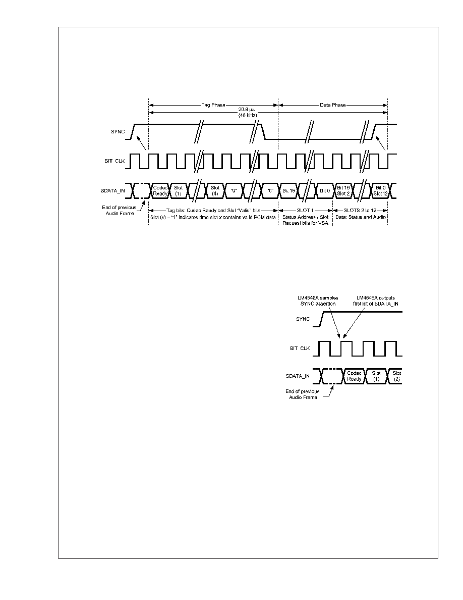
from the LM4546A codec. As shown in Figure 3, Input
Frames are constructed from thirteen time slots: one Tag
Slot followed by twelve Data Slots. The Tag Slot, Slot 0,
contains 16 bits of which 5 are used by the LM4546A. One is
used to indicate that the AC Link interface is fully operational
and the other 4 to indicate the validity of the data in the four
of the twelve following Data Slots that are used by the
LM4546A. Each Frame consists of 256 bits with each of the
twelve data slots containing 20 bits.
A new Input Frame is signaled with a low-to-high transition of
SYNC. SYNC should be clocked from the controller on a
rising edge of BIT_CLK and, as shown in Figure 6 and
Figure 7, the first tag bit in the Frame (“Codec Ready”) is
clocked from the LM4546A by the next rising edge of BIT-
_CLK. The LM4546A always clocks data to SDATA_IN on a
rising edge of BIT_CLK and the controller is expected to
sample SDATA_IN on the next falling edge. The LM4546A
samples SYNC on the rising edge of BIT_CLK.
Input and Output Frames are aligned to the same SYNC
transition.
The LM4546A checks each Frame to ensure 256 bits are
received. If a new Frame is detected (a low-to-high transition
on SYNC) before 256 bits are received from an old Frame
then the new Frame is ignored i.e. no valid data is sent on
SDATA_IN until a valid new Frame is detected.
The LM4546A transmits data MSB first, in a MSB justified
format. All reserved bits and slots are stuffed with "0"s by the
LM4546A.
SDATA_IN: Slot 0 – Codec/Slot Status Bits
The first bit (bit 15, “Codec Ready”) of slot 0 in the AC Link
Input Frame indicates when the codec’s AC Link digital
interface and its status/control registers are fully operational.
The digital controller is then able to read the LSBs from the
Powerdown Control/Stat register (26h) to determine the sta-
tus of the four main analog subsections. It is important to
check the status of these subsections after Initialization,
Cold Reset or the use of the powerdown modes in order to
minimize the risk of distorting analog signals passed before
the subsections are ready.
The 4 bits 14, 13, 12 and 11 indicate that the data in slots 1,
2, 3 and 4, respectively, are valid.
20030808
FIGURE 6. AC Link Input Frame
20030807
FIGURE 7. Start of AC Link Input Frame
LM4546A
www.national.com
18
相關(guān)PDF資料 |
PDF描述 |
|---|---|
| LM4546VHX | SPECIALTY CONSUMER CIRCUIT, PQFP48 |
| LM4546MDC | SPECIALTY CONSUMER CIRCUIT, UUC |
| LM4546MWC | SPECIALTY CONSUMER CIRCUIT, UUC |
| LM4546AVHX/NOPB | SPECIALTY CONSUMER CIRCUIT, PQFP48 |
| LM4546VH/NOPB | SPECIALTY CONSUMER CIRCUIT, PQFP48 |
相關(guān)代理商/技術(shù)參數(shù) |
參數(shù)描述 |
|---|---|
| LM4546AVHX | 制造商:Rochester Electronics LLC 功能描述:AC97 REV2 CODEC 3D STEREO - Bulk |
| LM4546B | 制造商:NSC 制造商全稱:National Semiconductor 功能描述:AC ’97 Rev 2 Multi-Channel Audio Codec with Sample Rate Conversion and National 3D Sound |
| LM4546BVH | 功能描述:接口—CODEC RoHS:否 制造商:Texas Instruments 類型: 分辨率: 轉(zhuǎn)換速率:48 kSPs 接口類型:I2C ADC 數(shù)量:2 DAC 數(shù)量:4 工作電源電壓:1.8 V, 2.1 V, 2.3 V to 5.5 V 最大工作溫度:+ 85 C 安裝風(fēng)格:SMD/SMT 封裝 / 箱體:DSBGA-81 封裝:Reel |
| LM4546BVH /NOPB | 制造商:Texas Instruments 功能描述:Audio Codec 2ADC / 2DAC 18-Bit 48-Pin LQFP Tray |
| LM4546BVH/NOPB | 功能描述:接口—CODEC RoHS:否 制造商:Texas Instruments 類型: 分辨率: 轉(zhuǎn)換速率:48 kSPs 接口類型:I2C ADC 數(shù)量:2 DAC 數(shù)量:4 工作電源電壓:1.8 V, 2.1 V, 2.3 V to 5.5 V 最大工作溫度:+ 85 C 安裝風(fēng)格:SMD/SMT 封裝 / 箱體:DSBGA-81 封裝:Reel |
發(fā)布緊急采購,3分鐘左右您將得到回復(fù)。