- 您現(xiàn)在的位置:買賣IC網 > PDF目錄361030 > LM556ICN Analog Timer Circuit PDF資料下載
參數資料
| 型號: | LM556ICN |
| 英文描述: | Analog Timer Circuit |
| 中文描述: | 模擬定時器電路 |
| 文件頁數: | 4/8頁 |
| 文件大小: | 216K |
| 代理商: | LM556ICN |
Electrical Characteristics
(Continued)
(T
A
= 25C, V
CC
= +5V to +15V, unless otherwise specified)
Parameter
Conditions
Limits
LM556C
Typ
12.5
13.3
3.3
100
100
Units
Min
Max
Output Voltage Drop (High)
I
SOURCE
= 200mA, V
CC
= 15V
I
SOURCE
= 100mA, V
CC
= 15V
V
CC
= 5V
V
V
V
ns
ns
12.75
2.75
Rise Time of Output
Fall Time of Output
Matching Characteristics
Initial Timing Accuracy
Timing Drift with Temperature
Drift with Supply Voltage
(Note 8)
0.1
±
10
0.2
2.0
%
ppm/C
%/V
0.5
Note 1:
Absolute Maximum Ratings indicate limits beyond which damage to the device may occur.
Note 2:
For operating at elevated temperatures the device must be derated based on a +150C maximum junction temperature and a thermal resistance of 77C/W
(Plastic Dip), and 110C/W (SO-14 Narrow).
Note 3:
Supply current when output high typically 1mA less at V
CC
= 5V.
Note 4:
Tested at V
CC
= 5V and V
CC
= 15V.
Note 5:
As reset voltage lowers, timing is inhibited and then the output goes low.
Note 6:
This will determine the maximum value of R
A
+ R
B
for 15V operation. The maximum total (R
A
+ R
B
) is 20 M
.
Note 7:
No protection against excessive pin 1, 13 current is necessary providing the package dissipation rating will not be exceeded.
Note 8:
Matching characteristics refer to the difference between performance characteristics of each timer section.
Note 9:
Refer to RETS556X drawing of military LM556J versions.
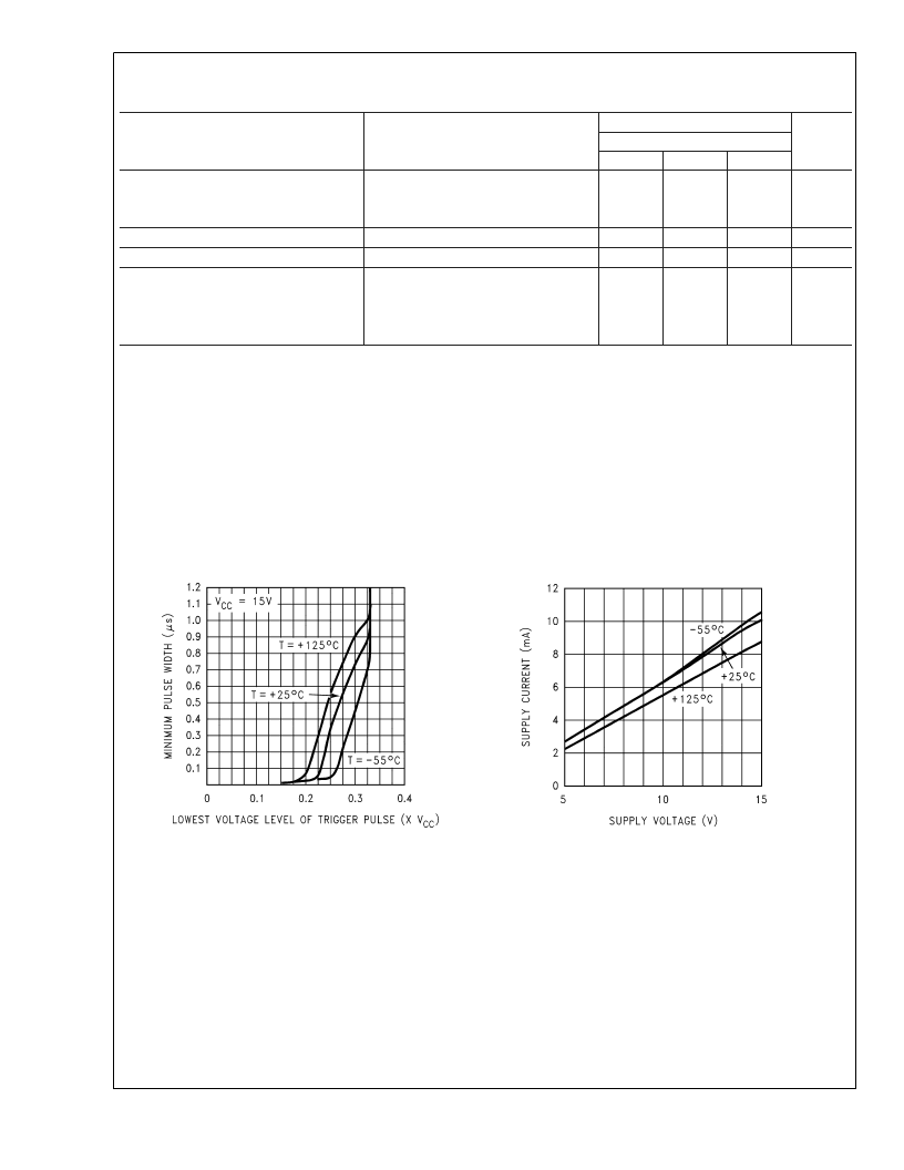
Typical Performance Characteristics
Minimum Pulse Width Required for Triggering
DS007852-3
Supply Current vs. Supply Voltage (Each Section)
DS007852-4
L
www.national.com
4
相關PDF資料 |
PDF描述 |
|---|---|
| LM556J-MIL | Analog Timer Circuit |
| LM556CIN | Analog Timer Circuit |
| LM556CM | Dual Timer |
| LM556CMX | Dual Timer |
| LM556CN | CAP 40V 470UF ELECT AXIAL |
相關代理商/技術參數 |
參數描述 |
|---|---|
| LM556J/A+ | 制造商:未知廠家 制造商全稱:未知廠家 功能描述:Analog Timer Circuit |
| LM556J-M1L | 制造商:IC'S/TRANSISTORS/DIO 功能描述: 制造商:IC'S/TRANSISTORS/DIODES 功能描述: |
| LM556J-MIL | 制造商:National Semiconductor Corporation 功能描述:Standard Timer Dual 14-Pin CDIP Rail |
| LM5574 | 制造商:NSC 制造商全稱:National Semiconductor 功能描述:75V, 0.5A Step-Down Switching Regulator |
| LM5574_09 | 制造商:NSC 制造商全稱:National Semiconductor 功能描述:SIMPLE SWITCHER 75V, 0.5A Step-Down Switching Regulator |
發(fā)布緊急采購,3分鐘左右您將得到回復。