- 您現(xiàn)在的位置:買賣IC網(wǎng) > PDF目錄358875 > LM79L12S Analog IC PDF資料下載
參數(shù)資料
| 型號(hào): | LM79L12S |
| 英文描述: | Analog IC |
| 中文描述: | 模擬IC |
| 文件頁(yè)數(shù): | 3/8頁(yè) |
| 文件大小: | 619K |
| 代理商: | LM79L12S |

Absolute Maximum Ratings
(Note 1)
If Military/Aerospace specified devices are required,
please contact the National Semiconductor Sales Office/
Distributors for availability and specifications.
Input Voltage
V
O
= 5V, 12V, 15V
Internal Power Dissipation (Note 2)
35V
Internally Limited
Operating Temperature Range
Maximum Junction Temperature
Storage Temperature Range
Lead Temperature
(Soldering, 10 sec.)
0C to +70C
+125C
55C to +150C
260C
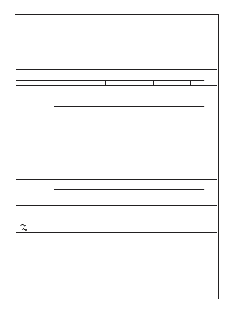
Electrical Characteristics
(Note 3)
T
A
= 0C to +70C unless otherwise noted.
Output Voltage
Input Voltage (unless otherwise noted)
Symbol
Parameter
V
O
Output
Voltage
1mA
≤
I
O
≤
100mA
V
MIN
≤
V
IN
≤
V
MAX
1mA
≤
I
O
≤
40mA
V
MIN
≤
V
IN
≤
V
MAX
V
O
Line
Regulation
V
MIN
≤
V
IN
≤
V
MAX
T
J
= 25C, I
O
= 40mA
V
MIN
≤
V
IN
≤
V
MAX
V
O
Load
Regulation
1mA
≤
I
O
≤
100mA
V
O
Long Term
Stability
I
Q
Quiescent
Current
I
Q
Quiescent
Current
Change
1mA
≤
I
O
≤
40mA
I
O
= 100mA
V
MIN
≤
V
IN
≤
V
MAX
V
n
Output Noise
Voltage
f = 10Hz 10kHz
Ripple
Rejection
f = 120Hz
5V
10V
Typ
5
12V
17V
Typ
12
15V
20V
Typ
15
Units
Conditions
Min
5.2
Max
4.8
Min
12.5
Max
11.5
Min
15.6
Max
14.4
T
J
= 25C, I
O
= 100mA
5.25
(20
≤
V
IN
≤
7.5)
5.25
(20
≤
V
IN
≤
7)
4.75
12.6
(27
≤
V
IN
≤
14.8)
12.6
(27
≤
V
IN
≤
14.5)
11.4
15.75
(30
≤
V
IN
≤
18)
15.75
(30
≤
V
IN
≤
17.5)
14.25
V
4.75
11.4
14.25
T
J
= 25C, I
O
= 100mA
60
45
45
mV
(20
≤
V
IN
≤
7.3)
(27
≤
V
IN
≤
14.6)
(30
≤
V
IN
≤
17.7)
V
60
45
45
mV
V
(20
≤
V
IN
≤
7)
(27
≤
V
IN
≤
14.5)
(30
≤
V
IN
≤
17.5)
T
J
= 25C
50
100
125
mV
I
O
= 100mA
20
48
60
mV/khrs
I
O
= 100mA
2
6
2
6
2
6
mA
1mA
≤
I
O
≤
100mA
0.3
0.3
0.3
0.1
0.25
0.1
0.25
0.1
0.25
mA
mA
V
(20
≤
V
IN
≤
7.5)
(27
≤
V
IN
≤
14.8)
(30
≤
V
IN
≤
18)
T
J
= 25C, I
O
= 100mA
40
96
120
μV
T
J
= 25C, I
O
= 100mA
50
52
50
dB
Input Voltage T
J
= 25C, I
O
= 100mA
Required to
I
O
= 40mA
Maintain Line
Regulation
7.3
7.0
14.6
14.5
17.7
17.5
V
V
Note 1:
Absolute Maximum Ratings indicate limits beyond which damage to the device may occur. Operating Ratings indicate conditions for which the device is
functional, but do not guarantee specific performance limits.
Note 2:
Thermal resistance of Z package is 60C/W
θ
, 232C/W
θ
at still air, and 88C/W at 400 ft/min of air. The M package
θ
JA
is 180C/W in still air. The
maximum junction temperature shall not exceed 125C on electrical parameters.
Note 3:
To ensure constant junction temperature, low duty cycle pulse testing is used.
L
www.national.com
3
相關(guān)PDF資料 |
PDF描述 |
|---|---|
| LM79L12T | Analog IC |
| LM79L15S | Analog IC |
| LM79L15T | Analog IC |
| LM79L18 | Analog IC |
| LM79L18S | Analog IC |
相關(guān)代理商/技術(shù)參數(shù) |
參數(shù)描述 |
|---|---|
| LM79L12T | 制造商:未知廠家 制造商全稱:未知廠家 功能描述:Analog IC |
| LM79L12TA | 制造商:HTC 制造商全稱:HTC Korea TAEJIN Technology Co. 功能描述:3-TERMINAL 0.1A NEGATIVE VOLTAGE REGULATOR |
| LM79L13ACM | 制造商:NSC 制造商全稱:National Semiconductor 功能描述:3-Terminal Negative Regulators |
| LM79L13ACMX | 制造商:NSC 制造商全稱:National Semiconductor 功能描述:3-Terminal Negative Regulators |
| LM79L15 | 制造商:IC'S/TRANSISTORS/DIO 功能描述: 制造商:IC'S/TRANSISTORS/DIODES 功能描述: |
發(fā)布緊急采購(gòu),3分鐘左右您將得到回復(fù)。