- 您現(xiàn)在的位置:買賣IC網(wǎng) > PDF目錄361035 > LM9800CCV (NATIONAL SEMICONDUCTOR CORP) 8-Bit Greyscale/24-Bit Color Linear CCD Sensor Processor PDF資料下載
參數(shù)資料
| 型號: | LM9800CCV |
| 廠商: | NATIONAL SEMICONDUCTOR CORP |
| 元件分類: | 模擬信號調(diào)理 |
| 英文描述: | 8-Bit Greyscale/24-Bit Color Linear CCD Sensor Processor |
| 中文描述: | SPECIALTY ANALOG CIRCUIT, PQCC52 |
| 封裝: | PLASTIC, LCC-52 |
| 文件頁數(shù): | 26/34頁 |
| 文件大小: | 619K |
| 代理商: | LM9800CCV |
第1頁第2頁第3頁第4頁第5頁第6頁第7頁第8頁第9頁第10頁第11頁第12頁第13頁第14頁第15頁第16頁第17頁第18頁第19頁第20頁第21頁第22頁第23頁第24頁第25頁當前第26頁第27頁第28頁第29頁第30頁第31頁第32頁第33頁第34頁
Applications Information
(Continued)
4.3 GAIN (VGA) Input
The LM9800 has a VGA(Variable GainAmplifier) that can be
used to increase the amplitude of the CCD signal prior to
sampling, correction, and digitization. In a greyscale system,
the VGA can provide gain for all the pixels. The VGA is acti-
vated or bypassed by setting or resetting the
VGA
bit in the
configuration register. For greyscale systems using the VGA,
the VGA bit and all 3
Pixel Gain
bits (VGA
a
, VGA
b
, and
VGA
c
) should be set to “1”.
The gain of the VGA is determined by the voltage on the
GAIN input as given by the equation:
Where V
is the voltage at the GAIN input of the LM9800.
A detailed graph of this function is provided in the
Typical
Performance Characteristics
section of the datasheet.
This equation is accurate for the V
voltage range of 0.5V
to 2.0V, corresponding to a gain range of x1.5 to x2.7 (typi-
cal).
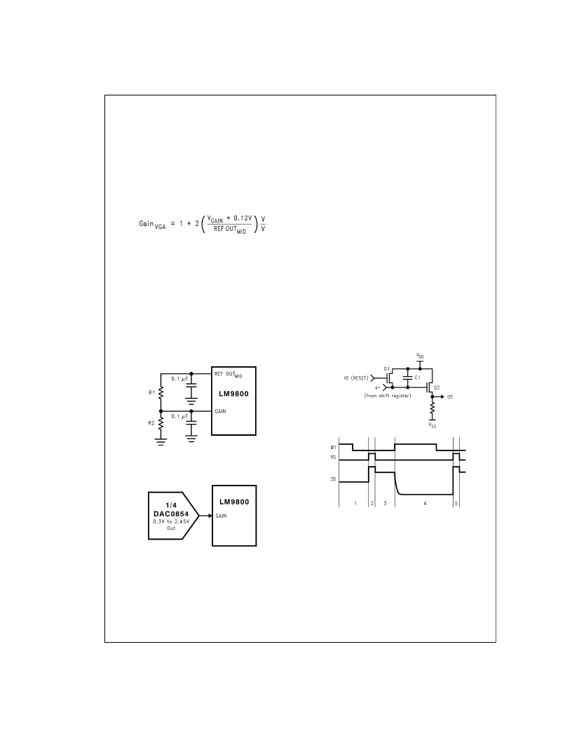
The voltage at the GAIN input may be supplied by a resistive
divider between REF OUT
and AGND or by a voltage out-
put DAC. The divider provides a low cost fixed gain suitable
for many applications. The DAC allows fine, closed-loop ad-
justment of the gain which can eliminate system-to-system
CCD gain and light source intensity variations to maximize
dynamic range. The DAC0854 has the ideal output voltage
range for this application and requires no additional external
components.
If the VGA is not going to be used, the GAIN input should be
tied to AGND.
4.4 Color Gain Switching
The VGA can also be used in color LM9800-based systems
with sequential (serial) color CCD outputs (RGBRG-
BRGB. . .). Sequential RGB color CCDs typically have a
Blue signal that is substantially lower (30%–70%) in ampli-
tude than the Red and Green signals. The LM9800 can com-
pensate for this by allowing the VGA to be turned on and off
at the pixel rate, allowing each pixel in a three pixel triad to
have one of two different gains (see Figure 13 VGA Gain
Switching). When the VGA is bypassed, the gain through the
VGAstage is 1. When the VGAis activated, the gain through
the VGA stage is determined by the external voltage on the
GAIN input. The Configuration Register controls whether or
not gain switching is implemented, and which pixels are
routed through the VGA.
Gain switching is controlled by the VGA On/Off bit and the
three Pixel Gain bits in the Configuration Register. If the VGA
On/Off bit is set to 0, then the VGA is bypassed (a gain of 1)
for all pixels. If the VGA On/Off bit is set to 1, then the gain
for each pixel inside every three pixel “triad” is set by the
VGA State for Pixel “n”
bits. For example, if the CCD out-
put data is RGBRGBRGB, then the VGA state bits in the
configuration register should be 001 (Pixel “a” = 0, Pixel “b”
= 0, Pixel “c” = 1). The VGA would then be bypassed for the
Red and Green pixels (for an effective gain of 1), and the
Blue pixels would be routed through the VGA for amplifica-
tion (as determined by the voltage on the GAIN input). Note
that the VGA is always off (for an effective gain of 1) for the
first pixel immediately following the last optical black pixel,
regardless of the setting of the gain bit.
Other color configurations are described in section 5.0.
4.5 Correlated Double Sampler (CDS)
Figure 33 shows the output stage of a typical CCD and the
resulting output waveform:
Capacitor C1 converts the electrons coming from the CCD’s
shift register to an analog voltage. The source follower out-
put stage (Q2) buffers this voltage before it leaves the CCD.
Q1 resets the voltage across capacitor C1 in between every
pixel at intervals 2 and 5. When Q1 is on, the output signal
(OS) is at its maximum. After Q1 turns off (period 3), the OS
level represents the residual voltage across C1 (V
).
V
includes charge injection from Q1, thermal noise
from the ON resistance of Q1, and other sources of error.
When the shift register clock (
φ
1) makes a low to high tran-
sition (period 4), the electrons from the next pixel flow into
C1. The charge across C1 now contains the voltage propor-
tional to the number of electrons plus V
RESIDUAL
, an error
DS012498-37
Note :
10 k
≤
R1 + R2
≤
50 k
FIGURE 31. GAIN Control with Voltage Divider
DS012498-38
FIGURE 32. GAIN Control with DAC
DS012498-39
DS012498-40
FIGURE 33. CDS
www.national.com
26
相關(guān)PDF資料 |
PDF描述 |
|---|---|
| LM9811CCVF | 10-Bit Greyscale/30-Bit Color Linear CCD Sensor Processor |
| LM9811 | 10-Bit Greyscale/30-Bit Color Linear CCD Sensor Processor |
| LM9811CCV | 10-Bit Greyscale/30-Bit Color Linear CCD Sensor Processor |
| LM9831CCVJD | LM9831 42-Bit Color, 1200dpi USB Image Scanner |
| LM9831 | LM9831 42-Bit Color, 1200dpi USB Image Scanner |
相關(guān)代理商/技術(shù)參數(shù) |
參數(shù)描述 |
|---|---|
| LM9800CCVF | 制造商:未知廠家 制造商全稱:未知廠家 功能描述:Special Function Video Processor |
| LM9801 | 制造商:NSC 制造商全稱:National Semiconductor 功能描述:Greyscale/24-Bit Color Linear CCD Sensor Processor |
| LM9801CCV | 制造商:NSC 制造商全稱:National Semiconductor 功能描述:Greyscale/24-Bit Color Linear CCD Sensor Processor |
| LM9801CCVF | 制造商:NSC 制造商全稱:National Semiconductor 功能描述:Greyscale/24-Bit Color Linear CCD Sensor Processor |
| LM980-SC3 | 功能描述:基本/快動開關(guān) Foot Switch RoHS:否 制造商:Omron Electronics 觸點形式:SPDT 執(zhí)行器:Lever 電流額定值:5 A 電壓額定值 AC:250 V 電壓額定值 DC:30 V 功率額定值: 工作力:120 g IP 等級:IP 67 NEMA 額定值: 端接類型:Wire 安裝:Panel |
發(fā)布緊急采購,3分鐘左右您將得到回復。