- 您現(xiàn)在的位置:買賣IC網(wǎng) > PDF目錄377649 > LMA2010 (Logic Devices Incorporated) 16 x 16-Bit Multiplier-Accumulator(16x 16位乘法器-累加器) PDF資料下載
參數(shù)資料
| 型號: | LMA2010 |
| 廠商: | Logic Devices Incorporated |
| 英文描述: | 16 x 16-Bit Multiplier-Accumulator(16x 16位乘法器-累加器) |
| 中文描述: | 16 × 16位乘法累加器(16x的16位乘法器-累加器) |
| 文件頁數(shù): | 5/7頁 |
| 文件大小: | 192K |
| 代理商: | LMA2010 |
DEVICES INCORPORATED
LMA1010/2010
16 x 16-bit Multiplier-Accumulator
Multiplier-Accumulators
08/16/2000–LDS.10/2010-P
5
1. Maximum Ratings indicate stress
specifications only. Functional oper-
ation of these products at values beyond
those indicated in the Operating Condi-
tions table is not implied. Exposure to
maximum rating conditions for ex-
tended periods may affect reliability.
2. The products described by this spec-
ification include internal circuitry de-
signed to protect the chip from damag-
ing substrate injection currents and ac-
cumulations of static charge. Neverthe-
less, conventional precautions should
be observed during storage, handling,
and use of these circuits in order to
avoid exposure to excessive electrical
stress values.
3. This device provides hard clamping of
transient undershoot and overshoot. In-
put levels below ground or above
V
CC
will be clamped beginning at –0.6 V and
V
CC
+ 0.6 V. The device can withstand
indefinite operation with inputs in the
range of –0.5 V to +7.0 V. Device opera-
tion will not be adversely affected, how-
ever, input current levels will be well in
excess of 100 mA.
4. Actual test conditions may vary from
those designated but operation is guar-
anteed as specified.
5. Supply current for a given applica-
tion can be accurately approximated by:
where
N = total number of device outputs
C = capacitive load per output
V = supply voltage
F = clock frequency
6. Tested with all outputs changing ev-
ery cycle and no load, at a 5 MHz clock
rate.
7. Tested with all inputs within 0.1 V of
V
CC
or Ground, no load.
8. These parameters are guaranteed
but not 100% tested.
NCV F
4
NOTES
9. AC specifications are tested with
input transition times less than 3 ns,
output reference levels of 1.5 V (except
t
DIS
test), and input levels of nominally
0 to 3.0 V. Output loading may be a
resistive divider which provides for
specified
I
OH
and
I
OL
at an output
voltage of
V
OH
min and
V
OL
max
respectively. Alternatively, a diode
bridge with upper and lower current
sources of
I
OH
and
I
OL
respectively,
and a balancing voltage of 1.5 V may be
used. Parasitic capacitance is 30 pF
minimum, and may be distributed.
This device has high-speed outputs ca-
pable of large instantaneous current
pulses and fast turn-on/turn-off times.
As a result, care must be exercised in the
testing of this device. The following
measures are recommended:
a. A 0.1 μF ceramic capacitor should be
installed between
V
CC
and Ground
leads as close to the Device Under Test
(DUT) as possible. Similar capacitors
should be installed between device
V
CC
and the tester common, and device
ground and tester common.
b. Ground and
V
CC
supply planes
must be brought directly to the DUT
socket or contactor fingers.
c. Input voltages should be adjusted to
compensate for inductive ground and
V
CC
noise to maintain required DUT input
levels relative to the DUT ground pin.
10. Each parameter is shown as a min-
imum or maximum value. Input re-
quirements are specified from the point
of view of the external system driving
the chip. Setup time, for example, is
specified as a minimum since the exter-
nal system must supply at least that
much time to meet the worst-case re-
quirements of all parts. Responses from
the internal circuitry are specified from
the point of view of the device. Output
delay, for example, is specified as a
maximum since worst-case operation of
any device always provides data within
that time.
11. For the
t
ENA
test, the transition is
measured to the 1.5 V crossing point
with datasheet loads. For the
t
DIS
test,
the transition is measured to the
±200mV level from the measured
steady-state output voltage with
±10mA loads. The balancing volt-
age, V
TH
, is set at 3.5 V for Z-to-0
and 0-to-Z tests, and set at 0 V for Z-
to-1 and 1-to-Z tests.
12. These parameters are only tested at
the high temperature extreme, which is
the worst case for leakage current.
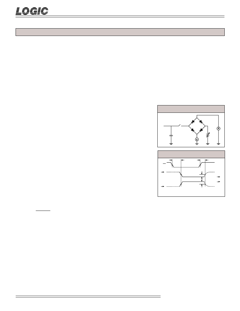
S1
I
OH
I
OL
V
TH
C
L
DUT
OE
0.2 V
t
DIS
t
ENA
0.2 V
1.5 V
1.5 V
3.5V Vth
1
Z
0
Z
Z
1
Z
0
1.5 V
1.5 V
0V Vth
V
OL
*
V
OH
*
V
OL
*
V
OH
*
Measured V
OL
with I
OH
= –10mA and I
OL
= 10mA
Measured V
OH
with I
OH
= –10mA and I
OL
= 10mA
F
IGURE
B. T
HRESHOLD
L
EVELS
F
IGURE
A. O
UTPUT
L
OADING
C
IRCUIT
相關(guān)PDF資料 |
PDF描述 |
|---|---|
| LMBD2835LT1G | Monolithic Dual Switching Diodes |
| LMBD2835LT3G | Monolithic Dual Switching Diodes |
| LMBD2836LT1G | Monolithic Dual Switching Diodes |
| LMBD2836LT3G | Monolithic Dual Switching Diodes |
| LMBD2837LT1 | Monolithic Dual Switching Diodes |
相關(guān)代理商/技術(shù)參數(shù) |
參數(shù)描述 |
|---|---|
| LMA2010JC20 | 制造商:未知廠家 制造商全稱:未知廠家 功能描述:Multiplier/Accumulator |
| LMA2010JC25 | 制造商:LOGIC 制造商全稱:LOGIC 功能描述:16 x 16-bit Multiplier-Accumulator |
| LMA2010JC35 | 制造商:LOGIC 制造商全稱:LOGIC 功能描述:16 x 16-bit Multiplier-Accumulator |
| LMA2010JC45 | 制造商:未知廠家 制造商全稱:未知廠家 功能描述:Multiplier/Accumulator |
| LMA2010JC55 | 制造商:未知廠家 制造商全稱:未知廠家 功能描述:Multiplier/Accumulator |
發(fā)布緊急采購,3分鐘左右您將得到回復(fù)。