- 您現(xiàn)在的位置:買(mǎi)賣(mài)IC網(wǎng) > PDF目錄384602 > LMC272 (National Semiconductor Corporation) CMOS Dual Low Cost Rail to Rail Output Operational Amplifier PDF資料下載
參數(shù)資料
| 型號(hào): | LMC272 |
| 廠商: | National Semiconductor Corporation |
| 英文描述: | CMOS Dual Low Cost Rail to Rail Output Operational Amplifier |
| 中文描述: | CMOS雙低成本軌至軌輸出運(yùn)算放大器 |
| 文件頁(yè)數(shù): | 7/16頁(yè) |
| 文件大?。?/td> | 458K |
| 代理商: | LMC272 |
第1頁(yè)第2頁(yè)第3頁(yè)第4頁(yè)第5頁(yè)第6頁(yè)當(dāng)前第7頁(yè)第8頁(yè)第9頁(yè)第10頁(yè)第11頁(yè)第12頁(yè)第13頁(yè)第14頁(yè)第15頁(yè)第16頁(yè)
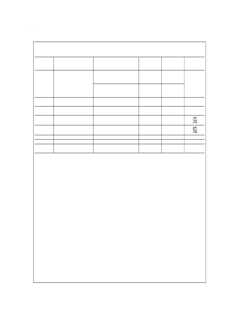
10V AC Electrical Characteristics
Unless otherwise specified, all limits guaranteed for T
= 25C, V
+
= 10V, V
= 0V, V
CM
= V
O
= V
+
/2, R
L
to ground and R
L
>
1 M
.
Boldface
limits apply at the temperature extremes
Typ
LMC272C
Limit
(Note 6)
Symbol
Parameter
Conditions
(Note 5)
Units
SR
Slew Rate (Note 8)
A
V
= +1, R
L
= 10 k
,
VI = 1 V
PP
, C
L
= 20 pF
(Note 12)
A
V
= +1, R
L
= 10 k
,
VI = 5.5 V
PP
, C
L
= 20 pF
(Note 12)
VI = 10 mV, C
L
= 20 pF
(Note 12)
VI = 10 mV, C
L
= 20 pF
(Note 12)
f = 1 kHz, R
S
= 20
V/μs
2.65
2.65
GBW
Unity Gain Frequency
2.1
MHz
φ
m
Phase Margin
44
Deg
e
n
Input-Referred
25
Voltage Noise
i
n
Input-Referred
f = 1 kHz
0.0015
Current Noise
f
max
Full Power Bandwidth
Amp-to-Amp Isolation
Total Harmonic
Distortion
C
L
= 20 pF, R
L
= 20 k
(Note 9)
A
V
= +1, V
IN
= 5 V
PP
f = 1 kHz
120
150
0.005
kHz
dB
%
THD
Note 1:
Absolute Maximum Ratings indicate limits beyond which damage to the device may occur. Operating Ratings indicate conditions for which the device is in-
tended to be functional, but specific performance is not guaranteed. For guaranteed specifications and the test conditions, see the Electrical characteristics.
Note 2:
Human body model, 1.5 k
in series with 100 pF.
Note 3:
Applies to both single-supply and split-supply operation. Continuous short circuit operation at elevated ambient temperature can result in exceeding the
maximum allowed junction temperature of 150C. Output currents in excess of
±
30 mA over long term may adversely affect reliability.
Note 4:
The maximum power dissipation is a function of T
,
θ
, and T
A
. The maximum allowable power dissipation at any ambient temperature is P
D
=(T
J(max)
T
A
)/
θ
JA
. All numbers apply for packages soldered directly into a PC board.
Note 5:
Typical Values represent the most likely parametric norm.
Note 6:
All limits are guaranteed by testing or statistical analysis.
Note 7:
Do not short circuit output to V+, when V+ is greater than 13V or reliability will be adversely affected.
Note 8:
Slew rate is the slower of the rising and falling slew rates.
Note 9:
Input referred, V+ = 10V and R
L
= 100 k
connected to 5V. Each amp excited in turn with 1 kHz to produce about 10 V
PP
output.
Note 10:
Limiting input pin current is only necessary for input voltages that exceed absolute maximum input voltage ratings.
Note 11:
V
ID
is the differential voltage on the non-inverting input with respect to the inverting input.
Note 12:
V
I
is the input voltage.
www.national.com
7
相關(guān)PDF資料 |
PDF描述 |
|---|---|
| LMC272CM | CMOS Dual Low Cost Rail to Rail Output Operational Amplifier |
| LMC272CMM | CMOS Dual Low Cost Rail to Rail Output Operational Amplifier |
| LMC272CMMX | CMOS Dual Low Cost Rail to Rail Output Operational Amplifier |
| LMC272CMX | CMOS Dual Low Cost Rail to Rail Output Operational Amplifier |
| LMC272CN | CMOS Dual Low Cost Rail to Rail Output Operational Amplifier |
相關(guān)代理商/技術(shù)參數(shù) |
參數(shù)描述 |
|---|---|
| LMC272BJE WAF | 制造商:Texas Instruments 功能描述: |
| LMC272CM | 制造商:NSC 制造商全稱(chēng):National Semiconductor 功能描述:CMOS Dual Low Cost Rail to Rail Output Operational Amplifier |
| LMC272CMM | 制造商:NSC 制造商全稱(chēng):National Semiconductor 功能描述:CMOS Dual Low Cost Rail to Rail Output Operational Amplifier |
| LMC272CMMX | 制造商:NSC 制造商全稱(chēng):National Semiconductor 功能描述:CMOS Dual Low Cost Rail to Rail Output Operational Amplifier |
| LMC272CMX | 制造商:NSC 制造商全稱(chēng):National Semiconductor 功能描述:CMOS Dual Low Cost Rail to Rail Output Operational Amplifier |
發(fā)布緊急采購(gòu),3分鐘左右您將得到回復(fù)。