- 您現(xiàn)在的位置:買賣IC網(wǎng) > PDF目錄361036 > LMC6022IM (NATIONAL SEMICONDUCTOR CORP) Low Power CMOS Dual Operational Amplifier PDF資料下載
參數(shù)資料
| 型號(hào): | LMC6022IM |
| 廠商: | NATIONAL SEMICONDUCTOR CORP |
| 元件分類: | 運(yùn)算放大器 |
| 英文描述: | Low Power CMOS Dual Operational Amplifier |
| 中文描述: | DUAL OP-AMP, 11000 uV OFFSET-MAX, 0.35 MHz BAND WIDTH, PDSO8 |
| 封裝: | SO-8 |
| 文件頁數(shù): | 8/16頁 |
| 文件大?。?/td> | 339K |
| 代理商: | LMC6022IM |
Application Hints
(Continued)
ing load resistance of 5 k
or less, the gain will be reduced
as indicated in the Electrical Characteristics. The op amp
can drive load resistance as low as 500
without instability.
COMPENSATING INPUT CAPACITANCE
Refer to the LMC660 or LMC662 datasheets to determine
whether or not a feedback capacitor will be necessary for
compensation and what the value of that capacitor would be.
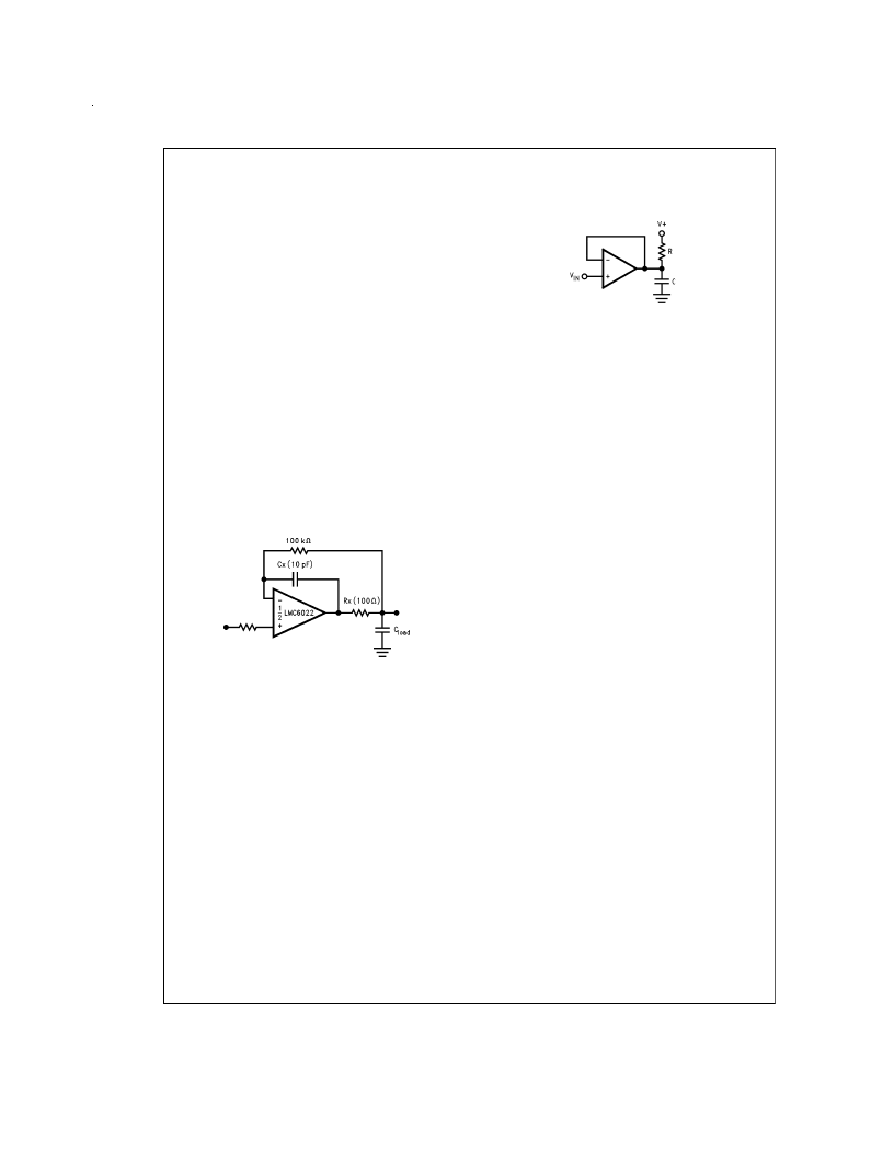
CAPACITIVE LOAD TOLERANCE
Like many other op amps, the LMC6022 may oscillate when
its applied load appears capacitive. The threshold of oscilla-
tion varies both with load and circuit gain. The configuration
most sensitive to oscillation is a unity-gain follower. See the
Typical Performance Characteristics.
The load capacitance interacts with the op amp’s output re-
sistance to create an additional pole. If this pole frequency is
sufficiently low, it will degrade the op amp’s phase margin so
that the amplifier is no longer stable at low gains. The addi-
tion of a small resistor (50
to 100
) in series with the op
amp’s output, and a capacitor (5 pF to 10 pF) from inverting
input to output pins, returns the phase margin to a safe value
without interfering with lower-frequency circuit operation.
Thus, larger values of capacitance can be tolerated without
oscillation. Note that in all cases, the output will ring heavily
when the load capacitance is near the threshold for
oscillation.
Capacitive load driving capability is enhanced by using a pull
up resistor to V
+
(Figure 3). Typically a pull up resistor con-
ducting 50 μA or more will significantly improve capacitive
load responses. The value of the pull up resistor must be de-
termined based on the current sinking capability of the ampli-
fier with respect to the desired output swing. Open loop gain
of the amplifier can also be affected by the pull up resistor
(see Electrical Characteristics).
PRINTED-CIRCUIT-BOARD LAYOUT
FOR HIGH-IMPEDANCE WORK
It is generally recognized that any circuit which must operate
with less than 1000 pA of leakage current requires special
layout of the PC board. When one wishes to take advantage
of the ultra-low bias current of the LMC6022, typically less
than 0.04 pA, it is essential to have an excellent layout. For-
tunately, the techniques for obtaining low leakages are quite
simple. First, the user must not ignore the surface leakage of
the PC board, even though it may sometimes appear accept-
ably low, because under conditions of high humidity or dust
or contamination, the surface leakage will be appreciable.
To minimize the effect of any surface leakage, lay out a ring
of foil completely surrounding the LMC6022’s inputs and the
terminals of capacitors, diodes, conductors, resistors, relay
terminals, etc. connected to the op-amp’s inputs. See Figure
4 To have a significant effect, guard rings should be placed
on both the top and bottom of the PC board. This PC foil
must then be connected to a voltage which is at the same
voltage as the amplifier inputs, since no leakage current can
flow between two points at the same potential. For example,
a PC board trace-to-pad resistance of 10
12
, which is nor-
mally considered a very large resistance, could leak 5 pA if
the trace were a 5V bus adjacent to the pad of an input. This
would cause a 100 times degradation from the LMC6022’s
actual performance. However, if a guard ring is held within
5 mV of the inputs, then even a resistance of 10
11
would
cause only 0.05 pA of leakage current, or perhaps a minor
(2:1) degradation of the amplifier’s performance. See Figure
5a Figure 5b Figure 5c for typical connections of guard
rings for standard op-amp configurations. If both inputs are
active and at high impedance, the guard can be tied to
ground and still provide some protection; see Figure 5d
DS011236-7
FIGURE 2. Rx, Cx Improve Capacitive Load Tolerance
DS011236-26
FIGURE 3. Compensating for Large
Capacitive Loads with a Pull Up Resistor
www.national.com
8
相關(guān)PDF資料 |
PDF描述 |
|---|---|
| LMC6022IN | Low Power CMOS Dual Operational Amplifier |
| LMC6024 | Low Power CMOS Quad Operational Amplifier |
| LMC6024IM | Low Power CMOS Quad Operational Amplifier |
| LMC6024IN | Low Power CMOS Quad Operational Amplifier |
| LMC6032 | CMOS Dual Operational Amplifier |
相關(guān)代理商/技術(shù)參數(shù) |
參數(shù)描述 |
|---|---|
| LMC6022IM/NOPB | 功能描述:運(yùn)算放大器 - 運(yùn)放 RoHS:否 制造商:STMicroelectronics 通道數(shù)量:4 共模抑制比(最小值):63 dB 輸入補(bǔ)償電壓:1 mV 輸入偏流(最大值):10 pA 工作電源電壓:2.7 V to 5.5 V 安裝風(fēng)格:SMD/SMT 封裝 / 箱體:QFN-16 轉(zhuǎn)換速度:0.89 V/us 關(guān)閉:No 輸出電流:55 mA 最大工作溫度:+ 125 C 封裝:Reel |
| LMC6022IMX | 功能描述:運(yùn)算放大器 - 運(yùn)放 RoHS:否 制造商:STMicroelectronics 通道數(shù)量:4 共模抑制比(最小值):63 dB 輸入補(bǔ)償電壓:1 mV 輸入偏流(最大值):10 pA 工作電源電壓:2.7 V to 5.5 V 安裝風(fēng)格:SMD/SMT 封裝 / 箱體:QFN-16 轉(zhuǎn)換速度:0.89 V/us 關(guān)閉:No 輸出電流:55 mA 最大工作溫度:+ 125 C 封裝:Reel |
| LMC6022IMX/NOPB | 功能描述:運(yùn)算放大器 - 運(yùn)放 RoHS:否 制造商:STMicroelectronics 通道數(shù)量:4 共模抑制比(最小值):63 dB 輸入補(bǔ)償電壓:1 mV 輸入偏流(最大值):10 pA 工作電源電壓:2.7 V to 5.5 V 安裝風(fēng)格:SMD/SMT 封裝 / 箱體:QFN-16 轉(zhuǎn)換速度:0.89 V/us 關(guān)閉:No 輸出電流:55 mA 最大工作溫度:+ 125 C 封裝:Reel |
| LMC6022IN | 制造商:NSC 制造商全稱:National Semiconductor 功能描述:Low Power CMOS Dual Operational Amplifier |
| LMC6024 | 制造商:NSC 制造商全稱:National Semiconductor 功能描述:Low Power CMOS Quad Operational Amplifier |
發(fā)布緊急采購,3分鐘左右您將得到回復(fù)。