- 您現(xiàn)在的位置:買賣IC網(wǎng) > PDF目錄361036 > LMC6032IN (NATIONAL SEMICONDUCTOR CORP) CMOS Dual Operational Amplifier PDF資料下載
參數(shù)資料
| 型號(hào): | LMC6032IN |
| 廠商: | NATIONAL SEMICONDUCTOR CORP |
| 元件分類: | 運(yùn)動(dòng)控制電子 |
| 英文描述: | CMOS Dual Operational Amplifier |
| 中文描述: | DUAL OP-AMP, 9000 uV OFFSET-MAX, 1.4 MHz BAND WIDTH, PDIP8 |
| 封裝: | DIP-8 |
| 文件頁(yè)數(shù): | 7/13頁(yè) |
| 文件大小: | 291K |
| 代理商: | LMC6032IN |
第1頁(yè)第2頁(yè)第3頁(yè)第4頁(yè)第5頁(yè)第6頁(yè)當(dāng)前第7頁(yè)第8頁(yè)第9頁(yè)第10頁(yè)第11頁(yè)第12頁(yè)第13頁(yè)
Application Hints
(Continued)
where
is the amplifier’s low-frequency noise gain and GBW is the
amplifier’s
gain
bandwidth
low-frequency noise gain is represented by the formula
product.
An
amplifier’s
regardless of whether the amplifier is being used in an invert-
ing or non-inverting mode. Note that a feedback capacitor is
more likely to be needed when the noise gain is low and/or
the feedback resistor is large.
If the above condition is met (indicating a feedback capacitor
will probably be needed), and the noise gain is large enough
that:
the following value of feedback capacitor is recommended:
If
the feedback capacitor should be:
Note that these capacitor values are usually significantly
smaller than those given by the older, more conservative for-
mula:
Using the smaller capacitors will give much higher band-
width with little degradation of transient response. It may be
necessary in any of the above cases to use a somewhat
larger feedback capacitor to allow for unexpected stray ca-
pacitance, or to tolerate additional phase shifts in the loop, or
excessive capacitive load, or to decrease the noise or band-
width, or simply because the particular circuit implementa-
tion needs more feedback capacitance to be sufficiently
stable. For example, a printed circuit board’s stray capaci-
tance may be larger or smaller than the breadboard’s, so the
actual optimum value for C
may be different from the one
estimated using the breadboard. In most cases, the value of
C
should be checked on the actual circuit, starting with the
computed value.
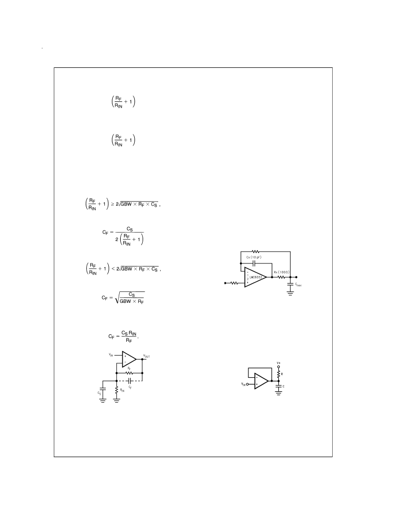
CAPACITIVE LOAD TOLERANCE
Like many other op amps, the LMC6032 may oscillate when
its applied load appears capacitive. The threshold of oscilla-
tion varies both with load and circuit gain. The configuration
most sensitive to oscillation is a unity-gain follower. See the
Typical Performance Characteristics.
The load capacitance interacts with the op amp’s output re-
sistance to create an additional pole. If this pole frequency is
sufficiently low, it will degrade the op amp’s phase margin so
that the amplifier is no longer stable at low gains. As shown
in Figure 3 the addition of a small resistor (50
to 100
) in
series with the op amp’s output, and a capacitor (5 pF to 10
pF) from inverting input to output pins, returns the phase
margin
to
a
safe
value
lower-frequency circuit operation. Thus, larger values of ca-
pacitance can be tolerated without oscillation. Note that in all
cases, the output will ring heavily when the load capacitance
is near the threshold for oscillation.
without
interfering
with
Capacitive load driving capability is enhanced by using a pull
up resistor to V
+
(Figure 4). Typically a pull up resistor con-
ducting 500 μA or more will significantly improve capacitive
load responses. The value of the pull up resistor must be de-
termined based on the current sinking capability of the ampli-
fier with respect to the desired output swing. Open loop gain
of the amplifier can also be affected by the pull up resistor
(see Electrical Characteristics).
PRINTED-CIRCUIT-BOARD LAYOUT
FOR HIGH-IMPEDANCE WORK
It is generally recognized that any circuit which must operate
with less than 1000 pA of leakage current requires special
layout of the PC board. When one wishes to take advantage
of the ultra-low bias current of the LMC6032, typically less
DS011135-4
S
consists of the amplifier’s input cacompensates for the pole caused by
C
F
C
S
and the feedback resistor.
FIGURE 2. General Operational Amplifier Circuit
DS011135-5
FIGURE 3. Rx, Cx Improve Capacitive Load Tolerance
DS011135-22
FIGURE 4. Compensating for Large Capacitive
Loads with a Pull Up Resistor
www.national.com
7
相關(guān)PDF資料 |
PDF描述 |
|---|---|
| LMC6061AIN | Precision CMOS Single Micropower Operational Amplifier |
| LMC6061AMN | Precision CMOS Single Micropower Operational Amplifier |
| LMC6061IM | Precision CMOS Single Micropower Operational Amplifier |
| LMC6061IN | Precision CMOS Single Micropower Operational Amplifier |
| LMC6061 | Precision CMOS Single Micropower Operational Amplifier |
相關(guān)代理商/技術(shù)參數(shù) |
參數(shù)描述 |
|---|---|
| LMC6032IN/NOPB | 功能描述:運(yùn)算放大器 - 運(yùn)放 CMOS Dual Op Amp RoHS:否 制造商:STMicroelectronics 通道數(shù)量:4 共模抑制比(最小值):63 dB 輸入補(bǔ)償電壓:1 mV 輸入偏流(最大值):10 pA 工作電源電壓:2.7 V to 5.5 V 安裝風(fēng)格:SMD/SMT 封裝 / 箱體:QFN-16 轉(zhuǎn)換速度:0.89 V/us 關(guān)閉:No 輸出電流:55 mA 最大工作溫度:+ 125 C 封裝:Reel |
| LMC6034 | 制造商:NSC 制造商全稱:National Semiconductor 功能描述:CMOS Quad Operational Amplifier |
| LMC6034IM | 功能描述:運(yùn)算放大器 - 運(yùn)放 RoHS:否 制造商:STMicroelectronics 通道數(shù)量:4 共模抑制比(最小值):63 dB 輸入補(bǔ)償電壓:1 mV 輸入偏流(最大值):10 pA 工作電源電壓:2.7 V to 5.5 V 安裝風(fēng)格:SMD/SMT 封裝 / 箱體:QFN-16 轉(zhuǎn)換速度:0.89 V/us 關(guān)閉:No 輸出電流:55 mA 最大工作溫度:+ 125 C 封裝:Reel |
| LMC6034IM/NOPB | 功能描述:運(yùn)算放大器 - 運(yùn)放 RoHS:否 制造商:STMicroelectronics 通道數(shù)量:4 共模抑制比(最小值):63 dB 輸入補(bǔ)償電壓:1 mV 輸入偏流(最大值):10 pA 工作電源電壓:2.7 V to 5.5 V 安裝風(fēng)格:SMD/SMT 封裝 / 箱體:QFN-16 轉(zhuǎn)換速度:0.89 V/us 關(guān)閉:No 輸出電流:55 mA 最大工作溫度:+ 125 C 封裝:Reel |
| LMC6034IM/NOPB | 制造商:Texas Instruments 功能描述:Operational Amplifier (Op-Amp) IC |
發(fā)布緊急采購(gòu),3分鐘左右您將得到回復(fù)。