- 您現(xiàn)在的位置:買賣IC網(wǎng) > PDF目錄367570 > LMC7211AIN IC-CMOS COMPARATOR PDF資料下載
參數(shù)資料
| 型號: | LMC7211AIN |
| 英文描述: | IC-CMOS COMPARATOR |
| 中文描述: | 集成電路的CMOS比較器 |
| 文件頁數(shù): | 4/14頁 |
| 文件大小: | 277K |
| 代理商: | LMC7211AIN |
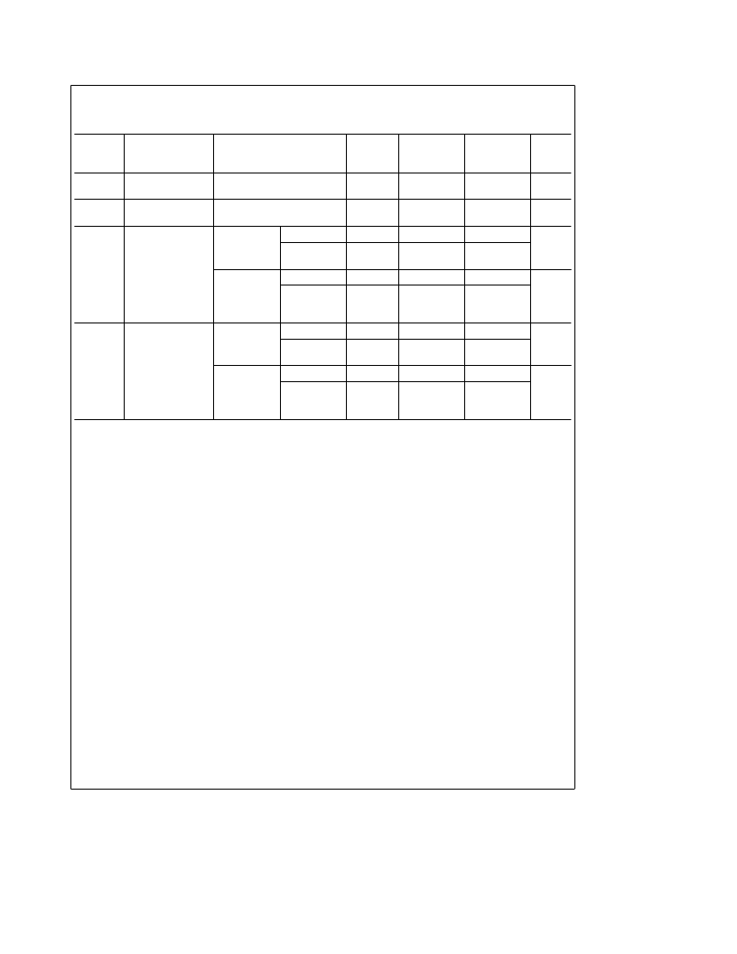
AC Electrical Characteristics
Unless otherwise specified, all limits guaranteed for T
J
e
25
§
C, V
a
e
5V, V
b
e
0V, V
CM
e
V
O
e
V
a
/2.
Boldface
limits
apply at the temperature extreme.
Typ
LMC7211AI
Limit
(Note 6)
LMC7211BI
Limit
(Note 6)
Symbol
Parameter
Conditions
(Note 5)
Units
t
rise
Rise Time
f
e
10 kHz, Cl
e
50 pF,
Overdrive
e
10 mV (Note 9)
0.3
m
s
t
fall
Fall Time
f
e
10 kHz, Cl
e
50 pF,
Overdrive
e
10 mV (Note 9)
0.3
m
s
t
PHL
Propagation Delay
(High to Low)
(Note 11)
f
e
10 kHz,
Cl
e
50 pF
(Note 9)
10 mV
10
m
s
100 mV
4
V
a e
2.7V,
f
e
10 kHz,
Cl
e
50 pF
(Note 9)
10 mV
10
m
s
100 mV
4
t
PLH
Propagation Delay
(Low to High)
(Note 11)
f
e
10 kHz,
Cl
e
50p
(Note 9)
10 mV
6
m
s
100 mV
4
V
a e
2.7V,
f
e
10 kHz,
Cl
e
50 pF
(Note 9)
10 mV
7
m
s
100 mV
4
Note 1:
Absolute Maximum Ratings indicate limits beyond which damage to the device may occur. Operating Ratings indicate conditions for which the device is
intended to be functional, but specific performance is not guaranteed. For guaranteed specifications and the test conditions, see the Electrical Characteristics.
Note 2:
Human body model, 1.5 k
X
in series with 100 pF.
Note 3:
Applies to both single-supply and split-supply operation. Continuous short circuit operation at elevated ambient temperature can result in exceeding the
maximum allowed junction temperature of 150
§
C. Output currents in excess of
g
30 mA over long term may adversely affect reliability.
Note 4:
The maximum power dissipation is a function of T
J(max)
,
i
JA
, and T
A
. The maximum allowable power dissipation at any ambient temperature is
P
D
e
(T
J(max)
b
T
A
)/
i
JA
. All numbers apply for packages soldered directly into a PC board.
Note 5:
Typical values represent the most likely parametric norm.
Note 6:
All limits are guaranteed by testing or statistical analysis.
Note 7:
Limiting input pin current is only necessary for input voltages that exceed absolute maximum input voltage rating.
Note 8:
Do not short circuit output to V
a
, when V
a
is greater than 12V or reliability will be adversely affected.
Note 9:
C
L
includes the probe and jig capacitance.
Note 10:
Input offset voltage average drift is calculated by dividing the accelerated operating life V
OS
drift by the equivalent operational time. This represents worst
case input conditions and includes the first 30 days of drift.
Note 11:
Input step voltage for propagation delay measurement is 2V.
4
相關PDF資料 |
PDF描述 |
|---|---|
| LMC7211BIN | IC-CMOS COMPARATOR R2R |
| LMC7225 | |
| LMC7532 | |
| LMC7660MJ | DC-to-DC Voltage Converter |
| LMF100AJ | Analog Filter |
相關代理商/技術參數(shù) |
參數(shù)描述 |
|---|---|
| LMC7211BIM | 功能描述:校驗器 IC RoHS:否 制造商:STMicroelectronics 產(chǎn)品: 比較器類型: 通道數(shù)量: 輸出類型:Push-Pull 電源電壓-最大:5.5 V 電源電壓-最小:1.1 V 補償電壓(最大值):6 mV 電源電流(最大值):1350 nA 響應時間: 最大工作溫度:+ 125 C 安裝風格:SMD/SMT 封裝 / 箱體:SC-70-5 封裝:Reel |
| LMC7211BIM | 制造商:Texas Instruments 功能描述:COMPARATOR RAIL/RAIL IP SMD 7211 |
| LMC7211BIM/NOPB | 功能描述:校驗器 IC Tiny CMOS Comparator RoHS:否 制造商:STMicroelectronics 產(chǎn)品: 比較器類型: 通道數(shù)量: 輸出類型:Push-Pull 電源電壓-最大:5.5 V 電源電壓-最小:1.1 V 補償電壓(最大值):6 mV 電源電流(最大值):1350 nA 響應時間: 最大工作溫度:+ 125 C 安裝風格:SMD/SMT 封裝 / 箱體:SC-70-5 封裝:Reel |
| LMC7211BIM5 | 功能描述:校驗器 IC RoHS:否 制造商:STMicroelectronics 產(chǎn)品: 比較器類型: 通道數(shù)量: 輸出類型:Push-Pull 電源電壓-最大:5.5 V 電源電壓-最小:1.1 V 補償電壓(最大值):6 mV 電源電流(最大值):1350 nA 響應時間: 最大工作溫度:+ 125 C 安裝風格:SMD/SMT 封裝 / 箱體:SC-70-5 封裝:Reel |
| LMC7211BIM5 | 制造商:Texas Instruments 功能描述:TINY CMOS COMP RAIL/RAIL IP 7211 |
發(fā)布緊急采購,3分鐘左右您將得到回復。