- 您現(xiàn)在的位置:買賣IC網(wǎng) > PDF目錄361043 > LMV7272 (National Semiconductor Corporation) Single & Dual, 1.8V Low Power Comparators with Rail-to-Rail Input PDF資料下載
參數(shù)資料
| 型號: | LMV7272 |
| 廠商: | National Semiconductor Corporation |
| 英文描述: | Single & Dual, 1.8V Low Power Comparators with Rail-to-Rail Input |
| 中文描述: | 單個 |
| 文件頁數(shù): | 10/16頁 |
| 文件大?。?/td> | 494K |
| 代理商: | LMV7272 |
Application Notes
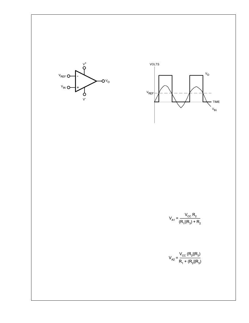
BASIC COMPARATOR
A comparator is often used to convert an analog signal to a
digital signal. As shown in
Figure 2
, the comparator com-
pares an input voltage (V
IN
) to a reference voltage (V
REF
). If
V
is less than V
REF
, the output (V
) is low. However, if V
IN
is greater than V
REF
, the output voltage (V
O
) is high.
RAIL-TO-RAIL INPUT STAGE
The LMV727X has an input common mode voltage range
(V
) of 0.1V below the V
to 0.1V above V
+
. This is
achieved by using paralleled PNP and NPN differential input
pairs. When the V
CM
is near V
+
, the NPN pair is on and the
PNP pair is off. When the V
CM
is near V
, the NPN pair is off
and the PNP pair is on. The crossover point between the
NPN and PNP input stages is around 950mV from V
+
. Since
each input stage has its own offset voltage (V
OS
), the V
OS
of
the comparator becomes a function of the V
CM
. See curves
for V
OS
vs. V
CM
in Typical Performance Characteristics sec-
tion. In application design, it is recommended to keep the
V
CM
away from the crossover point to avoid problems. The
wide input voltage range makes LMV727X ideal in power
supply monitoring circuits, where the comparators are used
to sense signals close to ground and power supplies.
OUTPUT STAGE
The LMV7271 and LMV7272 have a push-pull output stage.
This output stage keeps the total system power consumption
to the absolute minimum. The only current consumed is the
low supply current and the current going directly into the
load. When the output switches, both PMOS and NMOS at
the output stage are on at the same time for a very short
time. This allows current to flow directly between V
+
and V
through output transistors. The result is a short spike of
current (shoot-through current) drawn from the supply and
glitches in the supply voltages. The glitches can spread to
other parts of the board as noise. To prevent the glitches in
supply lines, power supply bypass capacitors must be in-
stalled. See section for supply bypassing in the Application
Notes for details.
HYSTERESIS
It is a standard procedure to use hysteresis (positive feed-
back) around a comparator, to prevent oscillation, and to
avoid excessive noise on the output because the comparator
is a good amplifier of its own noise.
Inverting Comparator with Hysteresis
The inverting comparator with hysteresis requires a three
resistor network that is referenced to the supply voltage V
CC
of the comparator (
Figure 3
). When V
IN
at the inverting input
is less than V
A
, the voltage at the non-inverting node of the
comparator (V
IN
<
V
A
), the output voltage is high (for sim-
plicity assume V
O
switches as high as V
CC
). The three
network resistors can be represented as R
||R
in series with
R
2
. The lower input trip voltage V
A1
is defined as
When V
is greater than V
(V
>
V
), the output voltage is
low and very close to ground. In this case the three network
resistors can be presented as R
//R
3
in series with R
1
. The
upper trip voltage V
A2
is defined as
The total hysteresis provided by the network is defined as
V
A
= V
A1
- V
A2
A good typical value of
V
would be in the range of 5 to
50mV. This is easily obtained by choosing R
as 1000 to 100
times (R
||R
) for 5V operation, or as 300 to 30 times
(R
1
||R
2
) for 1.8V operation.
LMV7271
20064025
20064017
FIGURE 2. LMV7271 Basic Comparator
L
www.national.com
10
相關(guān)PDF資料 |
PDF描述 |
|---|---|
| LMV7272TL | Single & Dual, 1.8V Low Power Comparators with Rail-to-Rail Input |
| LMV7272TLX | Single & Dual, 1.8V Low Power Comparators with Rail-to-Rail Input |
| LMV7275 | Single & Dual, 1.8V Low Power Comparators with Rail-to-Rail Input |
| LMV7275MF | Single & Dual, 1.8V Low Power Comparators with Rail-to-Rail Input |
| LMV7275MFX | Single & Dual, 1.8V Low Power Comparators with Rail-to-Rail Input |
相關(guān)代理商/技術(shù)參數(shù) |
參數(shù)描述 |
|---|---|
| LMV7272TL | 制造商:Texas Instruments 功能描述:Comparator Dual R-R I/P 5.5V 8-Pin uSMD T/R |
| LMV7272TL/NOPB | 功能描述:校驗(yàn)器 IC RoHS:否 制造商:STMicroelectronics 產(chǎn)品: 比較器類型: 通道數(shù)量: 輸出類型:Push-Pull 電源電壓-最大:5.5 V 電源電壓-最小:1.1 V 補(bǔ)償電壓(最大值):6 mV 電源電流(最大值):1350 nA 響應(yīng)時間: 最大工作溫度:+ 125 C 安裝風(fēng)格:SMD/SMT 封裝 / 箱體:SC-70-5 封裝:Reel |
| LMV7272TL-NOPB | 制造商:TI 制造商全稱:Texas Instruments 功能描述:Single & Dual, 1.8V Low Power Comparators with Rail-to-Rail Input |
| LMV7272TLX | 制造商:Texas Instruments 功能描述:Comparator Dual R-R I/P 5.5V 8-Pin uSMD T/R |
| LMV7272TLX/NOPB | 功能描述:校驗(yàn)器 IC RoHS:否 制造商:STMicroelectronics 產(chǎn)品: 比較器類型: 通道數(shù)量: 輸出類型:Push-Pull 電源電壓-最大:5.5 V 電源電壓-最小:1.1 V 補(bǔ)償電壓(最大值):6 mV 電源電流(最大值):1350 nA 響應(yīng)時間: 最大工作溫度:+ 125 C 安裝風(fēng)格:SMD/SMT 封裝 / 箱體:SC-70-5 封裝:Reel |
發(fā)布緊急采購,3分鐘左右您將得到回復(fù)。