- 您現(xiàn)在的位置:買賣IC網(wǎng) > PDF目錄383288 > LNBP21D2 (意法半導(dǎo)體) LNBP SUPPLY AND CONTROL IC WITH STEP-UP CONVERTER AND I2C INTERFACE PDF資料下載
參數(shù)資料
| 型號(hào): | LNBP21D2 |
| 廠商: | 意法半導(dǎo)體 |
| 英文描述: | LNBP SUPPLY AND CONTROL IC WITH STEP-UP CONVERTER AND I2C INTERFACE |
| 中文描述: | LNBP電源和控制集成電路升壓轉(zhuǎn)換器和I2C接口 |
| 文件頁數(shù): | 8/20頁 |
| 文件大小: | 693K |
| 代理商: | LNBP21D2 |
LNBP21
8/20
- no acknowledge, stopping the read mode
communication.
While the whole register is read back by the μP,
only the two read-only bits OLF and OTF convey
di-agnostic informations about the LNBP21.
Values are typical unless otherwise specified
POWER-ON I2C INTERFACE RESET
The
I2C
interface
automatically reset at power-on. As long as the
Vcc stays be-low the UnderVoltage Lockout
threshold (6.7V typ.), the interface will not respond
to any I2C com-mand and the System Register
(SR) is initialised to all zeroes, thus keeping the
power blocks disabled. Once the Vcc rises above
7.3V, the I2C interface becomes operative and the
SR can be configured by the main μP. This is due
to About 500mV of hysteresis provided in the UVL
threshold to avoid false
Power-On reset circuit.
built
in
the
LNBP21
is
retriggering
of the
DiSEqCTM IMPLEMENTATION
The LNBP21 helps the system designer to
implement the bi-directional (2.x) DiSEqC protocol
by
al-lowing
an
easy
demodulation of the 22KHz carrier. The PWK data
are exchanged between the LNBP21 and the
main μP using logic levels that are compatible with
both 3.3 and 5V mi-crocontrollers. This data
exchange is made through two dedicated pins,
DSQIN and DSQOUT, in or-der to maintain the
timing relationships between the PWK data and
the PWK modulation as accurate as possible.
These two pins should be directly connected to
two I/O pins of the μP, thus leaving to the resident
firmware the task of encoding and decoding the
PWK
modulation/
PWK data in accordance to the DiSEqC pro-tocol.
Full compliance of the system to the specification
is thus not implied by the bare use of the LNBP21.
The
system
designer
consideration the bus hardware requirements,
that include the source impedance of the Master
Transmitter measured at 22KHz. To limit the
attenuation at car-rier frequency, this impedance
has to be 15ohm at 22KHz, dropping to zero ohm
at DC to allow the power flow towards the
peripherals. This can be simply accomplished by
the LR
termination put on the OUT pin of the
LNBP, as shown in the Typical Application Circuit
on page 5.
Unidirectional (1.x) DiSEqC and non-DiSEqC
systems normally don't need this termination, and
the OUT pin can be directly connected to the LNB
supply port of the Tuner. There is also no need of
Tone Decoding, thus, it is recommended to
connect the DETIN and DSQOUT pins to ground
to avoid EMI.
should
also
take
in
ADDRESS PIN
Connecting this pin to GND the Chip I2C interface
address is 0001000, but, it is possible to choice
among 4 different addresses simply setting this
pin at 4 fixed voltage levels (see table on page
10).
ELECTRICALCHARACTERISTICS FOR LNBP SERIES
(T
J
= 0 to 85°C, EN=1, LLC=0,TEN=0, ISEL=0,
PCL=0, DSQIN=0, V
IN
=12V, I
OUT
=50mA, unless otherwise specified. See software description section
for I
2
C access to the system register)
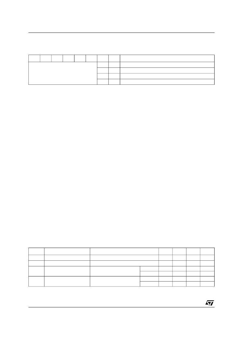
PCL
ISEL
TEN
LLC
VSEL
EN
OTF
OLF
Function
These bits are read exactly the same as
they were left after last write operation
0
1
T
J
<140°C, normal operation
T
J
>150°C, power block disabled, Loothrough switch open
I
OUT
<I
OMAX
, normal operation
I
OUT
>I
OMAX
, overload protection triggered
0
1
Symbol
Parameter
Test Conditions
Min.
Typ.
Max.
Unit
V
IN
V
LT1
I
IN
Supply Voltage
LT1 Input Voltage
Supply Current
I
O
= 500 mA TEN=VSEL=LLC=1
8
15
20
40
5
18.7
V
V
I
O
= 0mA TEN=VSEL=LLC=1
EN=1
EN=0
LLC=0
LLC=1
20
2.5
18
19
mA
mA
V
V
V
O
Output Voltage
I
O
= 500 mA VSEL=1
17.3
相關(guān)PDF資料 |
PDF描述 |
|---|---|
| LNBP21D2-TR | LNBP SUPPLY AND CONTROL IC WITH STEP-UP CONVERTER AND I2C INTERFACE |
| LNBP21PD | LNBP SUPPLY AND CONTROL IC WITH STEP-UP CONVERTER AND I2C INTERFACE |
| LNBS21PD-TR | SIGN, NO SMOKING, 175X125MM, SAV; RoHS Compliant: NA |
| LNBS21 | LNB SUPPLY AND CONTROL IC WITH STEP-UP CONVERTER AND I2C INTERFACE |
| LNBS21PD | LNB SUPPLY AND CONTROL IC WITH STEP-UP CONVERTER AND I2C INTERFACE |
相關(guān)代理商/技術(shù)參數(shù) |
參數(shù)描述 |
|---|---|
| LNBP21D2-TR | 功能描述:其他電源管理 LNB Supply/Control RoHS:否 制造商:Texas Instruments 輸出電壓范圍: 輸出電流:4 mA 輸入電壓范圍:3 V to 3.6 V 輸入電流: 功率耗散: 工作溫度范圍:- 40 C to + 110 C 安裝風(fēng)格:SMD/SMT 封裝 / 箱體:VQFN-48 封裝:Reel |
| LNBP21PD | 功能描述:其他電源管理 LNB Supply/Cont IC RoHS:否 制造商:Texas Instruments 輸出電壓范圍: 輸出電流:4 mA 輸入電壓范圍:3 V to 3.6 V 輸入電流: 功率耗散: 工作溫度范圍:- 40 C to + 110 C 安裝風(fēng)格:SMD/SMT 封裝 / 箱體:VQFN-48 封裝:Reel |
| LNBP21PD-TR | 功能描述:其他電源管理 LNB Supply/Cont IC RoHS:否 制造商:Texas Instruments 輸出電壓范圍: 輸出電流:4 mA 輸入電壓范圍:3 V to 3.6 V 輸入電流: 功率耗散: 工作溫度范圍:- 40 C to + 110 C 安裝風(fēng)格:SMD/SMT 封裝 / 箱體:VQFN-48 封裝:Reel |
| LNBP8 | 制造商:STMICROELECTRONICS 制造商全稱:STMicroelectronics 功能描述:LNB Supply and control voltage regulator |
| LNBP8_06 | 制造商:STMICROELECTRONICS 制造商全稱:STMicroelectronics 功能描述:LNB Supply and control voltage regulator |
發(fā)布緊急采購,3分鐘左右您將得到回復(fù)。