- 您現(xiàn)在的位置:買賣IC網(wǎng) > PDF目錄383288 > LNBS21PD (意法半導(dǎo)體) LNB SUPPLY AND CONTROL IC WITH STEP-UP CONVERTER AND I2C INTERFACE PDF資料下載
參數(shù)資料
| 型號(hào): | LNBS21PD |
| 廠商: | 意法半導(dǎo)體 |
| 英文描述: | LNB SUPPLY AND CONTROL IC WITH STEP-UP CONVERTER AND I2C INTERFACE |
| 中文描述: | LNB電源與控制集成電路升壓轉(zhuǎn)換器和I2C接口 |
| 文件頁(yè)數(shù): | 16/19頁(yè) |
| 文件大小: | 637K |
| 代理商: | LNBS21PD |
第1頁(yè)第2頁(yè)第3頁(yè)第4頁(yè)第5頁(yè)第6頁(yè)第7頁(yè)第8頁(yè)第9頁(yè)第10頁(yè)第11頁(yè)第12頁(yè)第13頁(yè)第14頁(yè)第15頁(yè)當(dāng)前第16頁(yè)第17頁(yè)第18頁(yè)第19頁(yè)
LNBS21
16/19
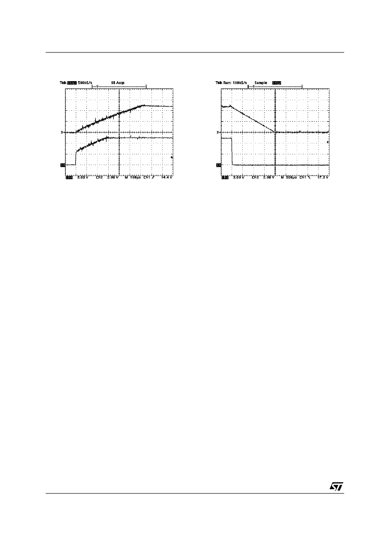
Figure 34 :
Output Voltage Transient Response
from 13V to 18V
Figure 35 :
Output Voltage Transient Response
from 13V to 18V
TERMAL DESIGN NOTES
During normal operation, this device dissipates
some power. At maximum rated output current
(500mA), the voltage drop on the linear regulator
lead to a total dissipated power that is of about
1.7W. The heat generated requires a suitable
heatsink to keep the junction temperature below
the
overtemperature
Assuming
a
40°C
temperature
Set-Top-Box case, the total Rthj-amb has to be
less than 50°C/W.
protection
threshold.
inside
the
While this
through-hole power package that can be attached
to a small heatsink or to the metallic frame of the
receiver, a surface mount power package must
rely on PCB solutions whose thermal efficiency is
often limited.
The simplest solution is to use a
large, con-tinuous copper area of the GND layer to
dissipate the heat coming from the IC body.
can be easily
achieved using a
The SO-20 package of this IC has 4 GND pins that
are
not
just
intended
connec-tion, but also to provide a low thermal
resistance path between the silicon chip and the
PCB heatsink. Given an Rthj-c equal to 15°C/W,
a maximum of
35°C/W
heatsink. This figure is achieved if a minimum of
25cm2 copper area is placed just below the IC
for
electrical
GND
are left to the PCB
body. This area can be the inner GND layer of a
multi-layer PCB, or, in a dual layer PCB, an
unbroken GND area even on the opposite side
where the IC is placed. In both cases, the thermal
path between the IC GND pins and the dissipating
copper area must exhibit a low thermal resistance.
In figure 4 , it is shown a suggested layout for the
SO-20 package with a dual layer PCB, where the
IC Ground pins and the square dissipating area
are thermally connected through 32 vias holes,
filled
by
solder.
This
L=50mm, achieves an Rthc-a of about 25°C/W.
Different
layouts
are
principles, however, suggest to keep the IC and its
ground pins approximately in the middle of the
dissipating area; to provide as many vias as
possible; to de-sign a dissipating area having a
shape as square as possible and not interrupted
by other copper traces.
Due to presence of an exposed pad connected to
GND below the IC
body, the PowerSO-20
package has a Rthj-c much lower than the SO-20,
only 2°C/W. As a result, much lower copper area
must be provided to dissipate the same power and
minimum of 12cm2 copper area is enough, see
figure 5.
arrangement,
when
possible,
too.
Basic
V
CC
=12V, I
O
=50mA, VSEL=from 0 to 1, EN=1
V
CC
=12V, I
O
=50mA, VSEL=from 1 to 0, EN=1
相關(guān)PDF資料 |
PDF描述 |
|---|---|
| LP1072 | 802.11a/b/g Baseband System Solution |
| LPR30 | LOW DROP VOLTAGE REGULATOR DRIVE FOR EXTERNAL N-CHANNEL POWER MOSFET |
| LPR30D | LOW DROP VOLTAGE REGULATOR DRIVE FOR EXTERNAL N-CHANNEL POWER MOSFET |
| LPR30D-TR | LOW DROP VOLTAGE REGULATOR DRIVE FOR EXTERNAL N-CHANNEL POWER MOSFET |
| LPR30N | LOW DROP VOLTAGE REGULATOR DRIVE FOR EXTERNAL N-CHANNEL POWER MOSFET |
相關(guān)代理商/技術(shù)參數(shù) |
參數(shù)描述 |
|---|---|
| LNBS21PD-TR | 功能描述:其他電源管理 LNB Supply/Cont IC RoHS:否 制造商:Texas Instruments 輸出電壓范圍: 輸出電流:4 mA 輸入電壓范圍:3 V to 3.6 V 輸入電流: 功率耗散: 工作溫度范圍:- 40 C to + 110 C 安裝風(fēng)格:SMD/SMT 封裝 / 箱體:VQFN-48 封裝:Reel |
| LNBTVS3-220 | 功能描述:TVS 二極管 - 瞬態(tài)電壓抑制器 3kV 1500W Ppp Lightning Protection RoHS:否 制造商:Vishay Semiconductors 極性:Bidirectional 工作電壓: 擊穿電壓:58.9 V 鉗位電壓:77.4 V 峰值浪涌電流:38.8 A 系列: 封裝 / 箱體:DO-214AB 最小工作溫度:- 55 C 最大工作溫度:+ 150 C |
| LNBTVS3-220S | 制造商:STMICROELECTRONICS 制造商全稱:STMicroelectronics 功能描述:Lightning protection for LNB power supply |
| LNBTVS3-220U | 功能描述:TVS 二極管 - 瞬態(tài)電壓抑制器 3kV 1500W Ppp Lightning Protection RoHS:否 制造商:Vishay Semiconductors 極性:Bidirectional 工作電壓: 擊穿電壓:58.9 V 鉗位電壓:77.4 V 峰值浪涌電流:38.8 A 系列: 封裝 / 箱體:DO-214AB 最小工作溫度:- 55 C 最大工作溫度:+ 150 C |
| LNBTVS3-221 | 制造商:STMICROELECTRONICS 制造商全稱:STMicroelectronics 功能描述:Lightning protection for LNB power supply |
發(fā)布緊急采購(gòu),3分鐘左右您將得到回復(fù)。