- 您現(xiàn)在的位置:買賣IC網(wǎng) > PDF目錄369842 > LSIFC929X LSIFC929X dual channel fibre solutions PDF資料下載
參數(shù)資料
| 型號: | LSIFC929X |
| 英文描述: | LSIFC929X dual channel fibre solutions |
| 中文描述: | LSIFC929X雙通道光纖解決方案 |
| 文件頁數(shù): | 52/144頁 |
| 文件大小: | 1496K |
| 代理商: | LSIFC929X |
第1頁第2頁第3頁第4頁第5頁第6頁第7頁第8頁第9頁第10頁第11頁第12頁第13頁第14頁第15頁第16頁第17頁第18頁第19頁第20頁第21頁第22頁第23頁第24頁第25頁第26頁第27頁第28頁第29頁第30頁第31頁第32頁第33頁第34頁第35頁第36頁第37頁第38頁第39頁第40頁第41頁第42頁第43頁第44頁第45頁第46頁第47頁第48頁第49頁第50頁第51頁當前第52頁第53頁第54頁第55頁第56頁第57頁第58頁第59頁第60頁第61頁第62頁第63頁第64頁第65頁第66頁第67頁第68頁第69頁第70頁第71頁第72頁第73頁第74頁第75頁第76頁第77頁第78頁第79頁第80頁第81頁第82頁第83頁第84頁第85頁第86頁第87頁第88頁第89頁第90頁第91頁第92頁第93頁第94頁第95頁第96頁第97頁第98頁第99頁第100頁第101頁第102頁第103頁第104頁第105頁第106頁第107頁第108頁第109頁第110頁第111頁第112頁第113頁第114頁第115頁第116頁第117頁第118頁第119頁第120頁第121頁第122頁第123頁第124頁第125頁第126頁第127頁第128頁第129頁第130頁第131頁第132頁第133頁第134頁第135頁第136頁第137頁第138頁第139頁第140頁第141頁第142頁第143頁第144頁
4-12
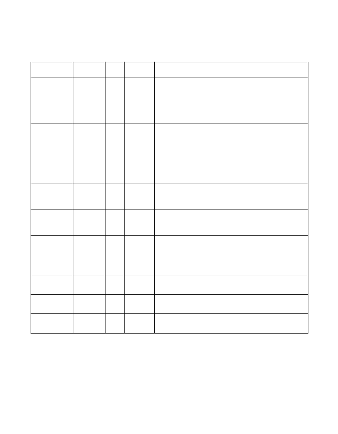
Signal Descriptions
Table 4.6
describes the Miscellaneous signals.
Table 4.6
Miscellaneous Signals
Name
BGA Pos
Type Strength Description
GPIO[3:0]
C12, B12,
A12, A13
I/O
8 mA
General purpose I/O pins.
These pins default to input
mode on reset. These signals are controlled/observed
by firmware and may be configured as inputs or
outputs. GPIO[3] may be optionally enabled as an
external interrupt source to the ARM RISC Processor
core. These pads contain an internal 100
μ
A pull-up.
LED[3:0]/
D11,
C11,
B11, A11
O
8 mA
LED Outputs.
These output signals may be controlled
by firmware or driven by chip activity. When configured
as activity driven, the LED[n] outputs have the following
meaning when asserted LOW:
LED[3]: Link Fault – Word Sync not detected
LED[2]: Receive Channel Active
LED[1]: Transmit Channel Active
LED[0]: Firmware controlled
SCL
A14
O
4 mA
Serial EEPROM clock.
This pad contains an internal
100
μ
A pull-up to provide a HIGH level on this pin, if it
is not used. If used, an external pull-up is also required.
SDA
B14
I/O
4 mA
Serial EEPROM data.
This pad contains an internal
100
μ
A pull-up to provide a HIGH level on this pin, if it
is not used. If used, an external pull-up is also required.
ZCLK
A6
I
N/A
External ZBus reference clock.
When FSELZ is held
LOW, this input pin provides the reference timing for the
internal ZBus, IOP and CtxMgr processors, and
memory interface. This pad contains an internal 100
μ
A
pull-up.
WmlsoTest[2]
B2
O
4 mA
Test mode output.
Leave unconnected. This pad
contains an internal 100
μ
A pull-up.
WmlsoTest[1]
A1
O
4 mA
Test mode output.
Leave unconnected. This pad
contains an internal 100
μ
A pull-up.
WmlsoTest[0]
A2
O
4 mA
Test mode output.
Leave unconnected. This pad
contains an internal 100
μ
A pull-up.
相關PDF資料 |
PDF描述 |
|---|---|
| LSIU160 | LSIU160 Ultra160 SCSI host adapter |
| LSIU40HVD | LSIU40HVD PCI to Dual Channel SCSI host adapter user's guide v2.2 8/02 |
| LSIU40SE | LSIU40SE Dual Channel PCI to Ultra SCSI host adapter user's guide v2.2 8/02 |
| LSIU80LVD | LSIU80LVD Ultra2 LVD SCSI host adapter |
| LSM615G | Schottky Rectifier |
相關代理商/技術(shù)參數(shù) |
參數(shù)描述 |
|---|---|
| LSIFC929XL | 制造商:LSI Corporation 功能描述:2GB PCI-X TO DUAL CHANNEL - Bulk |
| LSIFC949X | 制造商:LSI Corporation 功能描述:PCI-X TO DUAL CHANNEL - Bulk |
| LSIFC949X A0 | 制造商:LSI 功能描述: 制造商:LSI Corporation 功能描述: |
| LSIFC949X A1 | 制造商:LSI 功能描述: 制造商:LSI Corporation 功能描述: |
| LSIR3331 | 制造商:LIGITEK 制造商全稱:LIGITEK electronics co., ltd. 功能描述:INFRARED EMITTING DIODES |
發(fā)布緊急采購,3分鐘左右您將得到回復。