- 您現(xiàn)在的位置:買賣IC網(wǎng) > PDF目錄377666 > LT-94B73B-PW-AG (Optoway Technology Inc.) 3.3V / 2.488 Gbps 1490 nm Continuous-Mode TX PDF資料下載
參數(shù)資料
| 型號(hào): | LT-94B73B-PW-AG |
| 廠商: | Optoway Technology Inc. |
| 英文描述: | 3.3V / 2.488 Gbps 1490 nm Continuous-Mode TX |
| 中文描述: | 3.3 / 2.488 Gbps的1490納米連續(xù)模式得克薩斯州 |
| 文件頁(yè)數(shù): | 3/7頁(yè) |
| 文件大小: | 241K |
| 代理商: | LT-94B73B-PW-AG |
LT-94B73B-PWG
*****************************************************************************************************************************************************************************
Receiver Characteristics ( 0
o
C < Topr < 70
o
C, 3.13V < Vcc < 3.47V )
Parameter
Symbol
Min.
Optical
Sensitivity
Sen
Saturation Optical Power
Sat
-8
Wavelength of Operation
1260
Data Rate
1.244
Packet-to-Packet Guard Time
32
DC Optical Tolerance
Sen +3
Optical Return Loss
20
Signal Detect -- Asserted
Pa
Signal Detect -- Deasserted
Pd
-40
Signal detect -- Hysteresis
2
Electrical
Data Output Voltage
–
Low
V
OL
Vcc - 1.935
Data Output Voltage
–
High
V
OH
Vcc -1.135
Consecutive Identical Digit Immunity
72
Signal Detect Output Voltage -- Low
V
OL
Signal Detect Output Voltage -- High
V
OH
2.0
Signal Detect Assert Time
AS
MAX
10
Signal Detect Deassert Time
ANS
MAX
80
Received Power Monitoring Voltage
V
RPM
Rest Between Packet
2. Sensitivity and saturation levels at BER 1E-10 for a 2
23
-1 @ER=10.
3. At least 30 dB optical isolation for the wavelength 1480 to 1500 nm.
4. No reset is needed.
5. The optical power difference between neighboring packets is up to 15 dB.
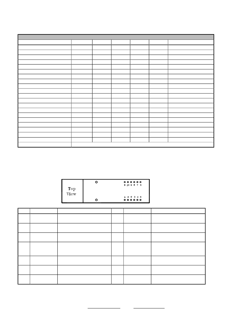
CONNECTION DIAGRAM
*****************************************************************************************************************************************************************************
OPTOWAY TECHNOLOGY INC.
No
.3
8, Kuang Fu S. Road, Hu Kou, Hsin Chu Industrial Park, Hsin Chu, Taiwan 303
Tel: 886-3-5979798 Fax: 886-3-5979737
E-mail: sales@optoway.com.tw http: // www.optoway.com.tw
5/1/2006 V1.0
3
Typ.
Max.
-28
1360
-28
Vcc - 1.56
Vcc - 0.76
0.5
30
150
Resetless
Units
dBm
dBm
nm
Gb/s
Bits
dB
dB
dBm
dBm
dB
V
V
Bits
V
V
ns
ns
V
Notes
2
2
3
4,5
Transition: low to high
Transition: high to low
15
100
Transition: low to high
Transition: high to low
Refer Figure 3.
PIN
A
Signal Name
RPM
Description
PIN
B
Signal Name
LF
Description
Receiver Power Monitor.
Laser failure warning out. This pin is
high when LD fails.
Negative transmitter data In. Internally
terminated for LVPECL. AC coupled.
Positive transmitter data In. Internally
terminated for LVPECL. AC coupled.
Transmitter Disable. TX is disabled
when this pin is low. Internally pulled
to
“
High
”
..
Transmitter Ground. Directly connect
this plan to ground plane
TX power supply input. Connect to 3.3
V power supply
1
RX Ground
Receiver Ground. Connect this pin to
ground plane.
RX power supply input. Connect to 3.3
V power supply
Signal Detect. High when single is
present (LVTTL)
10
TD-
2
RX Vcc
9
TD+
3
RX SD
8
TxDis
4
RX OUT (-)
Negative RX output, Differential
LVPECL. DC coupled.
Positive RX output, Differential
LVPECL. DC Coupled.
Mounting Studs. Connect to Chassis
Ground
7
TX Ground
5
RX OUT (+)
6
TX Vcc
MS
MS
相關(guān)PDF資料 |
PDF描述 |
|---|---|
| LT-94B73B-PWG | 3.3V / 2.488 Gbps 1490 nm Continuous-Mode TX |
| LT-94C73C-PWG | 3.3V / 2.488 Gbps 1490 nm Continuous-Mode TX |
| LT012S8 | Picoamp Input Current,Microvolt Offset,Low Noise Op Amp |
| LT1001ACJ8 | Circular Connector; MIL SPEC:MIL-DTL-38999 Series II; Body Material:Metal; Series:JT; No. of Contacts:10; Connector Shell Size:12; Connecting Termination:Crimp; Circular Shell Style:Straight Plug; Body Style:Straight RoHS Compliant: No |
| LT1001MJ8 | Precision Operational Amplifier |
相關(guān)代理商/技術(shù)參數(shù) |
參數(shù)描述 |
|---|---|
| LT-94B73B-PWG | 制造商:OPTOWAY 制造商全稱:Optoway Technology Inc 功能描述:3.3V / 2.488 Gbps 1490 nm Continuous-Mode TX |
| LT-94C73C-P1G | 制造商:OPTOWAY 制造商全稱:Optoway Technology Inc 功能描述:3.3V / 2.488 Gbps 1490 nm Continuous-Mode TX |
| LT-94C73C-PWG | 制造商:OPTOWAY 制造商全稱:Optoway Technology Inc 功能描述:3.3V / 2.488 Gbps 1490 nm Continuous-Mode TX |
| LT-950 | 制造商:Thomas & Betts 功能描述: |
| LT950-CAR | 制造商:Thomas & Betts 功能描述:1/2 BLACK 90 DEGREE LIQUIDTIGHT FT |
發(fā)布緊急采購(gòu),3分鐘左右您將得到回復(fù)。