- 您現(xiàn)在的位置:買賣IC網(wǎng) > PDF目錄377666 > LT1001C (Linear Technology Corporation) Precision Operational Amplifier PDF資料下載
參數(shù)資料
| 型號: | LT1001C |
| 廠商: | Linear Technology Corporation |
| 英文描述: | Precision Operational Amplifier |
| 中文描述: | 精密運(yùn)算放大器 |
| 文件頁數(shù): | 3/12頁 |
| 文件大?。?/td> | 326K |
| 代理商: | LT1001C |
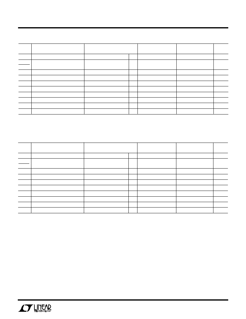
3
LT1001
ELECTRICAL CHARACTERISTICS
LT1001AM/883
MIN
TYP
30
0.2
LT1001M
TYP
45
0.3
SYMBOL PARAMETER
V
OS
Input Offset Voltage
V
OS
Average Offset Voltage Drift
Temp
I
OS
Input Offset Current
I
B
Input Bias Current
A
VOL
Large Signal Voltage Gain
CMRR
Common Mode Rejection Ratio
PSRR
Power Supply Rejection Ratio
Input Voltage Range
V
OUT
Output Voltage Swing
P
d
Power Dissipation
CONDITIONS
MAX
60
0.6
MIN
MAX
160
1.0
UNITS
G
μ
V
G
μ
V/
°
C
G
0.8
4.0
±
4.0
1.2
±
1.5
700
120
117
±
14
±
13.5
60
7.6
nA
nA
G
±
1.0
700
122
117
±
14
±
8.0
R
L
≥
2k
, V
O
=
±
10V
V
CM
=
±
13V
V
S
=
±
3 to
±
18V
G
300
110
104
±
13
±
12.5
±
13.5
200
106
100
±
13
±
12.0
V/mV
G
dB
dB
V
V
G
G
R
L
≥
2k
No load
G
G
55
90
100
mW
V
S
=
±
15V, –55
°
C
≤
T
A
≤
125
°
C, unless otherwise noted
LT1001AC
TYP
20
0.2
LT1001C
TYP
30
0.3
SYMBOL PARAMETER
V
OS
Input Offset Voltage
V
OS
Average Offset Voltage Drift
Temp
I
OS
Input Offset Current
I
B
Input Bias Current
A
VOL
Large Signal Voltage Gain
CMRR
Common Mode Rejection Ratio
PSRR
Power Supply Rejection Ratio
Input Voltage Range
V
OUT
Output Voltage Swing
P
d
Power Dissipation
CONDITIONS
MIN
MAX
60
0.6
MIN
MAX
110
1.0
UNITS
G
μ
V
G
μ
V/
°
C
G
0.5
3.5
±
3.5
0.6
±
1.0
750
123
120
±
14
±
13.8
55
5.3
±
5.5
nA
nA
G
±
0.7
750
124
120
±
14
R
L
≥
2k
, V
O
=
±
10V
V
CM
=
±
13V
V
S
=
±
3V to
±
18V
G
350
110
106
±
13
±
12.5
±
13.8
250
106
103
±
13
±
12.5
V/mV
G
dB
dB
V
V
G
G
R
L
≥
2k
No load
G
G
50
85
90
mW
The
G
denotes the specifications which apply over the full operating
temperature range.
Note 1:
Offset voltage for the LT1001AM/883 and LT1001AC are measured
after power is applied and the device is fully warmed up. All other grades
are measured with high speed test equipment, approximately 1 second
after power is applied. The LT1001AM/883 receives 168 hr. burn-in at
125
°
C. or equivalent.
Note 2:
This parameter is tested on a sample basis only.
Note 3:
Long Term Input Offset Voltage Stability refers to the averaged
trend line of V
OS
versus Time over extended periods after the first 30 days
of operation. Excluding the initial hour of operation, changes in V
OS
during
the first 30 days are typically 2.5
μ
V.
Note 4:
Parameter is guaranteed by design.
Note 5:
10Hz noise voltage density is sample tested on every lot. Devices
100% tested at 10Hz are available on request.
V
S
=
±
15V, 0
°
C
≤
T
A
≤
70
°
C, unless otherwise noted
相關(guān)PDF資料 |
PDF描述 |
|---|---|
| LT1001CH | Precision Operational Amplifier |
| LT1001CJ8 | Precision Operational Amplifier |
| LT1001CN8 | Precision Operational Amplifier |
| LT1001CS8 | Precision Operational Amplifier |
| LT1001MH | Precision Operational Amplifier |
相關(guān)代理商/技術(shù)參數(shù) |
參數(shù)描述 |
|---|---|
| LT1001CD | 制造商:Rochester Electronics LLC 功能描述:- Bulk |
| LT1001CDR | 制造商:Rochester Electronics LLC 功能描述:- Bulk |
| LT1001CH | 制造商:Linear Technology 功能描述:OP Amp Single GP ±22V 8-Pin TO-5 制造商:Linear Technology 功能描述:OP Amp Single GP 22V 8-Pin TO-5 |
| LT1001CJ8 | 制造商:Linear Technology 功能描述:OP Amp Single GP ±22V 8-Pin CDIP |
| LT1001CJG | 制造商:Rochester Electronics LLC 功能描述:- Bulk |
發(fā)布緊急采購,3分鐘左右您將得到回復(fù)。