- 您現(xiàn)在的位置:買賣IC網(wǎng) > PDF目錄377667 > LT1011MH (LINEAR TECHNOLOGY CORP) Voltage Comparator PDF資料下載
參數(shù)資料
| 型號(hào): | LT1011MH |
| 廠商: | LINEAR TECHNOLOGY CORP |
| 元件分類: | 運(yùn)動(dòng)控制電子 |
| 英文描述: | Voltage Comparator |
| 中文描述: | COMPARATOR, 3000 uV OFFSET-MAX, 150 ns RESPONSE TIME, MBCY8 |
| 封裝: | METAL CAN, TO-5, 8 PIN |
| 文件頁(yè)數(shù): | 3/16頁(yè) |
| 文件大小: | 205K |
| 代理商: | LT1011MH |
第1頁(yè)第2頁(yè)當(dāng)前第3頁(yè)第4頁(yè)第5頁(yè)第6頁(yè)第7頁(yè)第8頁(yè)第9頁(yè)第10頁(yè)第11頁(yè)第12頁(yè)第13頁(yè)第14頁(yè)第15頁(yè)第16頁(yè)

3
LT1011/LT1011A
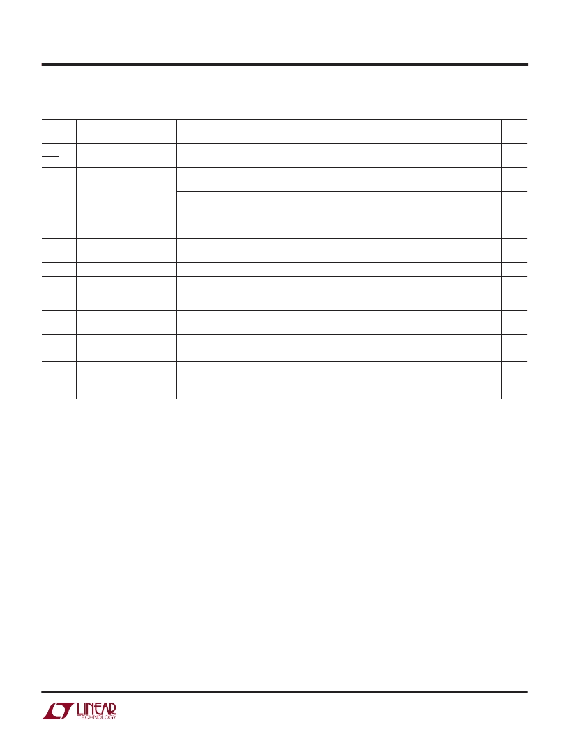
ELECTRICAL CHARACTERISTICS
The
G
denotes the specifications which apply over the full operating temperature range, otherwide specifications are at T
A
= 25
°
C.
V
S
=
±
15V, V
CM
= 0V, R
S
= 0
, V
1
= –15V, output at pin 7 unless otherwise noted.
SYMBOL
V
OS
T
A
VOL
PARAMETER
Input Offset Voltage Drift
(Note 6)
*Large-Signal Voltage Gain
CONDITIONS
T
MIN
≤
T
≤
T
MAX
MIN
TYP
4
MAX
15
MIN
TYP
4
MAX
25
UNITS
μ
V/
°
C
G
R
L
= 1k to 15V,
–10V
≤
V
OUT
≤
14.5V
R
L
= 500
to 5V,
0.5V
≤
V
OUT
≤
4.5V
200
500
200
500
V/mV
50
300
50
300
V/mV
CMRR
Common Mode
Rejection Ratio
*Input Voltage Range
(Note 9)
*Response Time
*Output Saturation Voltage,
V
1
= 0
94
115
90
115
dB
V
S
=
±
15V
V
S
= Single 5V
(Note 7)
V
IN
= 5mV, I
SINK
= 8mA, T
J
≤
100
°
C
V
IN
= 5mV, I
SINK
= 8mA
V
IN
= 5mV, I
SINK
= 50mA
V
IN
= 5mV, V
1
= –15V,
V
OUT
= 35V (25V for LT1011C/I)
G
G
–14.5
0.5
13
3
250
0.40
0.45
1.50
10
500
4.0
2.5
–14.5
0.5
13
3
250
0.40
0.45
1.50
10
500
4.0
2.5
V
V
t
D
V
OL
150
0.25
0.25
0.70
0.2
150
0.25
0.25
0.70
0.2
ns
V
V
V
nA
nA
mA
mA
μ
A
G
G
*Output Leakage Current
G
*Positive Supply Current
*Negative Supply Current
*Strobe Current
(Note 8)
Input Capacitance
3.2
1.7
3.2
1.7
Minimum to Ensure Output
Transistor is Off
500
500
6
6
pF
LT1011AC/AI/AM
LT1011C/I/M
Note 1:
Absolute Maximum Ratings are those values beyond which the
life of a device may be impaired.
Note 2:
Inputs may be clamped to supplies with diodes so that
maximum input voltage actually exceeds supply voltage by one diode
drop. See Input Protection in the Applications Information section.
Note 3:
T
JMAX
= 150
°
C.
Note 4:
Output is sinking 1.5mA with V
OUT
= 0V.
Note 5:
These specifications apply for all supply voltages from a single
5V to
±
15V, the entire input voltage range, and for both high and low
output states. The high state is I
SINK
≥
100
μ
A, V
OUT
≥
(V
+
– 1V) and
the low state is I
SINK
≤
8mA, V
OUT
≤
0.8V. Therefore, this specification
defines a worst-case error band that includes effects due to common
mode signals, voltage gain and output load.
Note 6:
Drift is calculated by dividing the offset voltage difference
measured at min and max temperatures by the temperature difference.
Note 7:
Response time is measured with a 100mV step and 5mV
overdrive. The output load is a 500
resistor tied to 5V. Time
measurement is taken when the output crosses 1.4V.
Note 8:
Do not short the STROBE pin to ground. It should be current
driven at 3mA to 5mA for the shortest strobe time. Currents as low as
500
μ
A will strobe the LT1011A if speed is not important. External
leakage on the STROBE pin in excess of 0.2
μ
A when the strobe is “off”
can cause offset voltage shifts.
Note 9:
See graph “Input Offset Voltage vs Common Mode Voltage.”
*
Indicates parameters which are guaranteed for all supply voltages, including a single 5V supply. See Note 5.
相關(guān)PDF資料 |
PDF描述 |
|---|---|
| LT1011AIS8 | Voltage Comparator |
| LT1012ACH | Picoamp Input Current, Microvolt Offset, Low Noise Op Amp |
| LT1012IS8 | Picoamp Input Current, Microvolt Offset, Low Noise Op Amp |
| LT1012MH | Picoamp Input Current, Microvolt Offset, Low Noise Op Amp |
| LT1012S8 | Picoamp Input Current, Microvolt Offset, Low Noise Op Amp |
相關(guān)代理商/技術(shù)參數(shù) |
參數(shù)描述 |
|---|---|
| LT1011MH/883C | 制造商:Linear Technology 功能描述: |
| LT1011MJ8 | 制造商:Linear Technology 功能描述:Comparator Single ±15V/30V 8-Pin CDIP |
| LT1011MJ8/883 | 制造商:Linear Technology 功能描述:Comparator Single ±15V/30V 8-Pin CDIP |
| LT1011MJG | 制造商:未知廠家 制造商全稱:未知廠家 功能描述:Analog Comparator |
| LT1011ML | 制造商:未知廠家 制造商全稱:未知廠家 功能描述:Analog Comparator |
發(fā)布緊急采購(gòu),3分鐘左右您將得到回復(fù)。