- 您現(xiàn)在的位置:買賣IC網(wǎng) > PDF目錄377668 > LT1019AMH-10 (LINEAR TECHNOLOGY CORP) Precision Reference PDF資料下載
參數(shù)資料
| 型號(hào): | LT1019AMH-10 |
| 廠商: | LINEAR TECHNOLOGY CORP |
| 元件分類: | 基準(zhǔn)電壓源/電流源 |
| 英文描述: | Precision Reference |
| 中文描述: | 1-OUTPUT THREE TERM VOLTAGE REFERENCE, 10 V, MBCY8 |
| 封裝: | METAL CAN, TO-5, 8 PIN |
| 文件頁數(shù): | 6/12頁 |
| 文件大?。?/td> | 158K |
| 代理商: | LT1019AMH-10 |
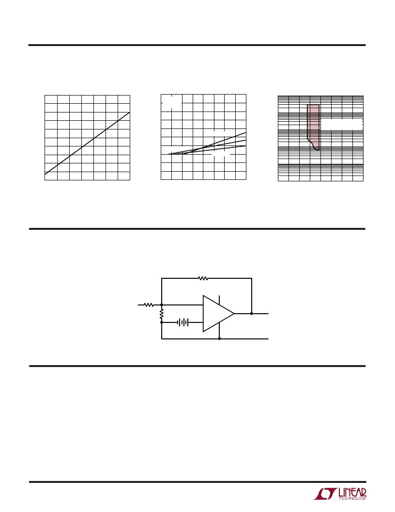
6
LT1019
C
HARA TERISTICS
U
A
TYPICAL PERFOR
CE
JUNCTION TEMPERATURE (
°
C)
–50
0.40
0.45
0.55
0.60
0.65
0.90
0.75
0
50
75
LT1019 TPC10
0.50
0.80
0.85
0.70
–25
25
100
125
Temp Pin Voltage
INPUT VOLTAGE (V)
0
–30
O
μ
V
–20
0
20
40
140
80
10
20
25
LT1019 TPC11
–10
100
120
60
5
15
30
35
40
LT1019-2.5
LT1019-5
I
OUT
T
J
= 25°C
LT1019-10
Line Regulation
LT1019-2.5* Stability with
Output Capacitance
*LT1019-4.5/LT1019-5/LT1019-10 ARE STABLE
WITH ALL LOAD CAPACITANCE.
OUTPUT CURRENT (mA)
0.01
O
μ
F
0.1
20
0
10
1019 G12
0.001
10
20
0.0001
1
10
15
SINK CURRENT
5
5
15
SOURCE CURRENT
REGION OF POSSIBLE
INSTABILITY
–
+
V
IN
1.188V
V
OUT
GND
R2
LT1019-4.5, LT1019-5,
LT1019-10 = 5k
LT1019-2.5 = 10k
R3
80k
TRIM
LT1019-2.5 = 11k
LT1019-4.5 = 13.9k
LT1019-5 = 16k
LT1019-10 = 37.1k
R1
LT1019 BD
BLOCK DIAGRAW
APPLICATIOU
Line and Load Regulation
U
W
U
Line regulation on the LT1019 is nearly perfect. A 10V
change in input voltage causes a typical output shift of less
than 5ppm. Load regulation (sourcing current) is nearly as
good. A 5mA change in load current shifts output voltage
by only 100
μ
V. These are electricaleffects, measured with
low duty cycle pulses to eliminate heating effects. In real
world applications, the thermaleffects of load and line
changes must be considered.
Two separate thermal effects are evident in monolithic
circuits. One is a gradient effect, where power dissipation
on the die creates temperature gradients. These gradients
can cause output voltage shifts even f the overall tempera-
ture coefficient of the reference s zero The LT1019, unlike
previous references, specifies thermal regulation caused
by die temperature gradients.The specification is
0.5ppm/mW. To calculate the effect on output voltage,
simply multiply the changein device power dissipation by
相關(guān)PDF資料 |
PDF描述 |
|---|---|
| LT1019-10 | Circular Connector; MIL SPEC:MIL-C-26482, Series I; Body Material:Aluminum Alloy; Series:MS3126; No. of Contacts:5; Connector Shell Size:14; Connecting Termination:Crimp; Circular Shell Style:Straight Plug RoHS Compliant: No |
| LT1019ACN8-2.5 | Precision Reference |
| LT1019CN8-2.5 | Precision Reference |
| LT1019IN8-2.5 | Precision Reference |
| LT1019ACS8-2.5 | Precision Reference |
相關(guān)代理商/技術(shù)參數(shù) |
參數(shù)描述 |
|---|---|
| LT1019AMH-10/883 | 制造商:Linear Technology 功能描述:V-Ref Precision 10V 10mA 8-Pin TO-5 |
| LT1019AMH-2.5 | 制造商:LINER 制造商全稱:Linear Technology 功能描述:Precision Reference |
| LT1019AMH-4.5 | 制造商:LINER 制造商全稱:Linear Technology 功能描述:Precision Reference |
| LT1019AMH-4.5/883 | 制造商:Linear Technology 功能描述:V-Ref Precision 4.5V 10mA 8-Pin TO-5 |
| LT1019AMH-5 | 制造商:LINER 制造商全稱:Linear Technology 功能描述:Precision Reference |
發(fā)布緊急采購,3分鐘左右您將得到回復(fù)。