- 您現(xiàn)在的位置:買賣IC網(wǎng) > PDF目錄383289 > LT119AH (LINEAR TECHNOLOGY CORP) Dual Comparator PDF資料下載
參數(shù)資料
| 型號: | LT119AH |
| 廠商: | LINEAR TECHNOLOGY CORP |
| 元件分類: | 運(yùn)動控制電子 |
| 英文描述: | Dual Comparator |
| 中文描述: | DUAL COMPARATOR, 1000 uV OFFSET-MAX, 80 ns RESPONSE TIME, MBCY10 |
| 封裝: | METAL CAN, TO-5, 10 PIN |
| 文件頁數(shù): | 3/8頁 |
| 文件大?。?/td> | 240K |
| 代理商: | LT119AH |
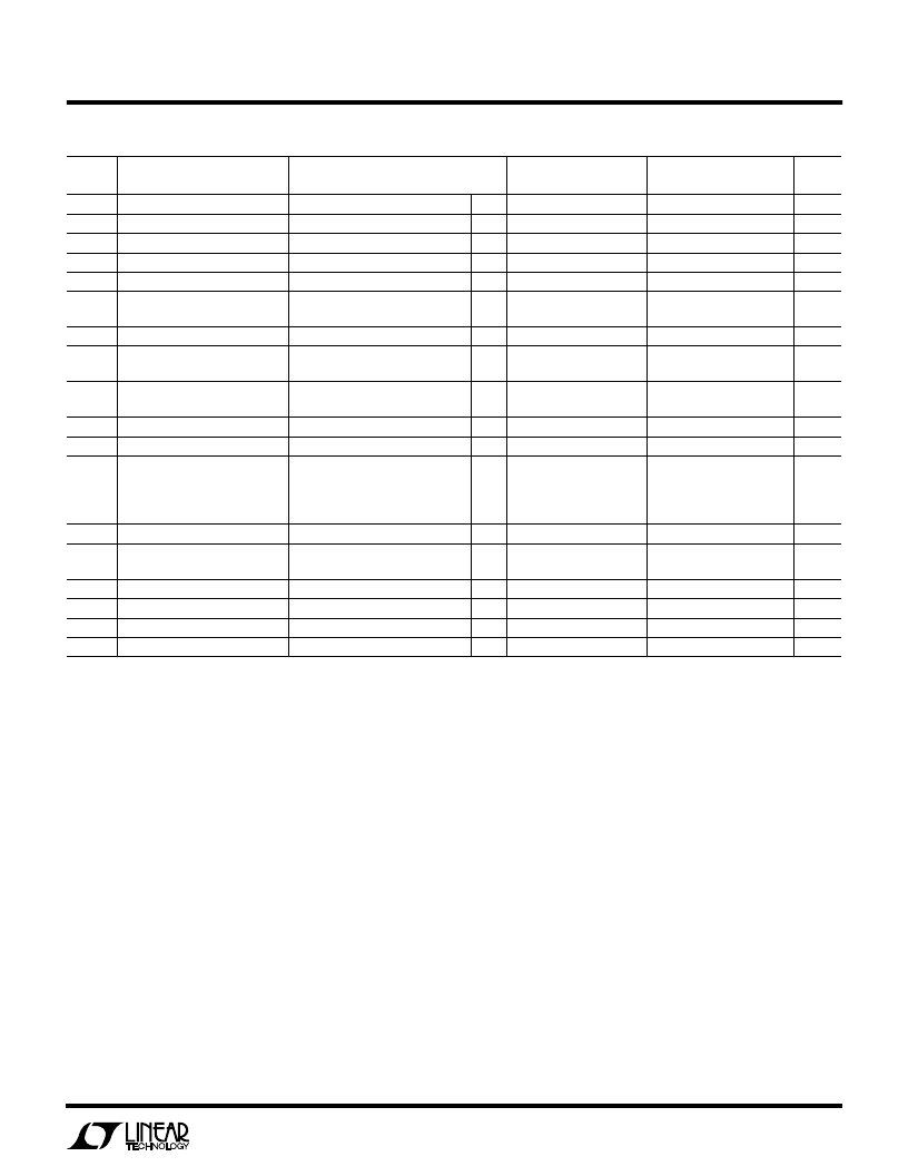
3
LT119A/LT319A
LM119/LM319
ELECTRICAL CHARACTERISTICS
(Note 2)
LT119A
TYP
LT119
TYP
SYMBOL
PARAMETER
Differential Input Voltage
Supply Current
Positive Supply Current
Negative Supply Current
Input Offset Voltage
Input Offset Voltage
CONDITIONS
MIN
MAX
±
5
MIN
MAX
±
5
UNITS
G
V
I
S
I
S
I
S
V
OS
V
OS
V
+
= 5V, V
–
= 0V
V
S
=
±
15V
V
S
=
±
15V
V
S
=
±
15V, V
CM
= 0V
R
S
≤
5k
(Note 3)
4.3
8
3
0.3
0.5
4.3
8
3
mA
mA
mA
mV
mV
mV
dB
nA
nA
nA
nA
11.5
4.5
0.5
1
2
11.5
4.5
8
8
10
2
G
CMRR
I
OS
Common-Mode Rejection Ratio
Input Offset Current
90
106
30
(Note 3)
40
60
500
1000
80
200
300
1000
1200
G
I
B
Input Bias Current
(Note 3)
150
250
G
A
V
Voltage Gain
Response Time
Saturation Voltage
20
40
80
8
40
80
V/mV
(Note 4)
V
IN
≤
–10mV, I
SINK
= 25mA
T
A
= 25
°
C
V
+
≥
4.5V, V
–
= 0V
V
IN
≤
–10mV, I
SINK
≤
3.2mA
V
IN
≥
10mV, V
OUT
= 35V
V
S
=
±
15V
V
+
= 5V, V
–
= 0V
ns
V
SAT
0.75
1.5
0.75
1.5
V
G
0.3
0.2
±
13
0.4
10
0.3
0.2
±
13
0.4
10
V
Output Leakage Current
Input Voltage Range
μ
A
V
V
V
mA
mA
mA
G
G
1
3
1
3
Differential Input Voltage
Supply Current
Positive Supply Current
Negative Supply Current
G
±
5
±
5
I
S
I
S
I
S
V
+
= 5V, V
–
= 0V
V
S
=
±
15V
V
S
=
±
15V
4.3
8
3
4.3
8
3
12.5
5
12.5
5
The
G
denotes specifications which apply over the full operating
temperature range.
Note 1:
For supply voltages less than
±
15V, the maximum input voltage is
equal to the supply voltage.
Note 2:
Unless otherwise noted, supply voltage equals
±
15V and
T
A
= 25
°
C. The ground pin is grounded. Note that the maximum voltage
allowed between the ground pin and V
+
is 18V. Do not tie the ground pin
to V
–
when the power supply voltage exceeds
±
9V. The offset voltage,
offset current and bias current specifications apply for all supply voltages
between
±
15V and 5V unless otherwise specified.
Note 3:
The offset voltages and currents given are the maximum values
required to drive the output within 1V of either supply with a 1mA load,
thus these parameters define an error band and take into account the
worst case effects of voltage gain and input impedance.
Note 4:
Response time specified is for a 100mV input step with 5mV
overdrive.
Note 5:
Inputs are protected with back-to-back 5.6V zener diodes. This
limits maximum differential input voltage to
±
5V if current is unlimited.
Larger differential input drive is allowed if input current is limited to
±
5mA
with external resistance.
相關(guān)PDF資料 |
PDF描述 |
|---|---|
| LT119AJ | Dual Comparator |
| LT3420 | Photoflash Capacitor Chargers with Automatic Refresh |
| LT3526 | Regulating Pulse Width Modulator |
| LT3526J | Regulating Pulse Width Modulator |
| LT3526N | Regulating Pulse Width Modulator |
相關(guān)代理商/技術(shù)參數(shù) |
參數(shù)描述 |
|---|---|
| LT11AF0911C | 制造商:Laird Technologies Inc 功能描述:CBS,OTH,NA,SLD / BP, / UOM=EA |
| LT11AF0911F | 制造商:Laird Technologies Inc 功能描述:CBS,OTH,NA,SLD / TnR, / UOM=EA |
| LT11AV3311 | 制造商:Laird Technologies Inc 功能描述:CSTR,PCS,SS,NID / .587X.315X0X.585IN / UOM=EA |
| LT11BC0651 | 制造商:Laird Technologies Inc 功能描述: |
| LT11BE0811 | 制造商:Laird Technologies Inc 功能描述: |
發(fā)布緊急采購,3分鐘左右您將得到回復(fù)。