- 您現(xiàn)在的位置:買賣IC網(wǎng) > PDF目錄377702 > LT1460S3-SOT-23 (Linear Technology Corporation) Family of Micropower Series References in SOT-23 PDF資料下載
參數(shù)資料
| 型號(hào): | LT1460S3-SOT-23 |
| 廠商: | Linear Technology Corporation |
| 英文描述: | Family of Micropower Series References in SOT-23 |
| 中文描述: | 家庭的微系列參考采用SOT - 23 |
| 文件頁數(shù): | 3/12頁 |
| 文件大小: | 287K |
| 代理商: | LT1460S3-SOT-23 |
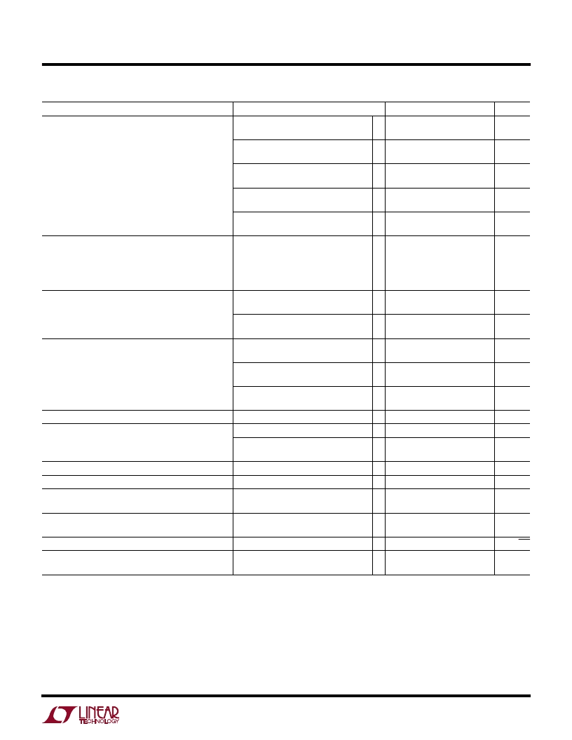
3
LT1460-10
PARAMETER
Output Voltage (Note 2)
CONDITIONS
LT1460ACN8, ACS8
MIN
9.9925
–0.075
9.990
–0.10
9.9875
–0.125
9.985
–0.15
9.975
–0.25
TYP
10.000
MAX
10.0075
0.075
10.010
0.10
10.0125
0.125
10.015
0.15
10.025
0.25
UNITS
V
%
V
%
V
%
V
%
V
%
LT1460BIN8, BIS8, CCMS8, DCN8, DCS8
10.000
LT1460EIN8, EIS8
10.000
LT1460FCMS8
10.000
LT1460GCZ, GIZ
10.000
Output Voltage Temperature Coefficient (Note 3)
T
MIN
≤
T
J
≤
T
MAX
LT1460ACN8, ACS8, BIN8, BIS8
LT1460CCMS8
LT1460DCN8, DCS8, EIN8, EIS8
LT1460FCMS8, GCZ, GIZ
10.9V
≤
V
IN
≤
12.5V
G
G
G
G
5
7
10
15
20
25
60
80
25
35
ppm/
°
C
ppm/
°
C
ppm/
°
C
ppm/
°
C
ppm/V
ppm/V
ppm/V
ppm/V
ppm/mA
ppm/mA
ppm/mA
ppm/mA
ppm/mA
ppm/mA
ppm/mW
10
12
30
Line Regulation
G
12.5V
≤
V
IN
≤
20V
10
G
Load Regulation Sourcing (Note 4)
I
OUT
= 100
μ
A
1500
2800
3500
135
180
100
140
2.5
0.9
1.3
1.4
G
I
OUT
= 10mA
80
G
I
OUT
= 20mA
0
°
C to 70
°
C
P = 200mW
V
IN
– V
OUT
,
V
OUT
≤
0.1%, I
OUT
= 0
V
IN
– V
OUT
,
V
OUT
≤
0.1%, I
OUT
= 10mA
70
G
Thermal Regulation (Note 5)
Dropout Voltage (Note 6)
0.5
G
V
V
V
G
Output Current
Reverse Leakage
Supply Current
Short V
OUT
to GND
V
IN
= –15V
40
0.5
190
mA
μ
A
μ
A
μ
A
G
10
270
360
G
Output Voltage Noise (Note 7)
0.1Hz
≤
f
≤
10Hz
10Hz
≤
f
≤
1kHz
40
35
40
160
25
μ
V
P-P
μ
V
RMS
Long-Term Stability of Output Voltage, S8 Pkg (Note 8)
Hysteresis (Note 9)
ppm/
√
kHr
T = –40
°
C to 85
°
C
T = 0
°
C to 70
°
C
ppm
ppm
The
G
denotes specifications which apply over the specified temperature
range.
Note 1:
If the part is stored outside of the specified temperature range, the
output may shift due to hysteresis.
Note 2:
ESD (Electrostatic Discharge) sensitive device. Extensive use of
ESD protection devices are used internal to the LT1460-10, however, high
electrostatic discharge can damage or degrade the device. Use proper ESD
handling precautions.
Note 3:
Temperature coefficient is measured by dividing the change in
output voltage by the specified temperature range. Incremental slope is
also measured at 25
°
C.
Note 4:
Load regulation is measured on a pulse basis from no load to the
specified load current. Output changes due to die temperature change
must be taken into account separately.
Note 5:
Thermal regulation is caused by die temperature gradients created
by load current or input voltage changes. This effect must be added to
normal line or load regulation. This parameter is not 100% tested.
ELECTRICAL CHARACTERISTICS
V
IN
= 12.5V, I
OUT
= 0, T
A
= 25
°
C unless otherwise specified.
相關(guān)PDF資料 |
PDF描述 |
|---|---|
| LT1460-2.5 | Micropower Precision Series Reference |
| LT1460GIZ-10 | Micropower Precision Series Reference |
| LT1460GIZ-2.5 | Micropower Precision Series Reference |
| LT1460GIZ-5 | Micropower Precision Series Reference |
| LT1460CCMS8-2.5 | Micropower Precision Series Reference |
相關(guān)代理商/技術(shù)參數(shù) |
參數(shù)描述 |
|---|---|
| LT1461 | 制造商:LINER 制造商全稱:Linear Technology 功能描述:Micropower Precision Low Dropout Series Voltage Reference Family |
| LT1461-2.5 | 制造商:LINER 制造商全稱:Linear Technology 功能描述:Serial 12-Bit/14-Bit, 2.8Msps |
| LT1461-3 | 制造商:LINER 制造商全稱:Linear Technology 功能描述:12-Bit, 5Msps Serial Sampling ADC in TSOT |
| LT1461-3.3V | 制造商:LINER 制造商全稱:Linear Technology 功能描述:12-Bit, 5Msps Serial Sampling ADC in TSOT |
| LT1461ACS8 | 制造商:LINER 制造商全稱:Linear Technology 功能描述:Micropower Precision Low Dropout Series Voltage Reference Family |
發(fā)布緊急采購,3分鐘左右您將得到回復(fù)。