- 您現(xiàn)在的位置:買賣IC網(wǎng) > PDF目錄383289 > LT5526 (Linear Technology Corporation) High Linearity, Low Power Downconverting Mixer PDF資料下載
參數(shù)資料
| 型號: | LT5526 |
| 廠商: | Linear Technology Corporation |
| 英文描述: | High Linearity, Low Power Downconverting Mixer |
| 中文描述: | 高線性度,低功耗下變頻混頻器 |
| 文件頁數(shù): | 11/16頁 |
| 文件大小: | 224K |
| 代理商: | LT5526 |
11
LT5526
5526f
The purpose of L5 is to provide a DC return path for Pin 3.
(Another possible placement for L5 would be across Pins
2 and 3, thus using L1 as part of the DC return path.) The
inductance and resonant frequency of L5 should be large
enough that they don’t significantly affect the input imped-
ance and performance of the balun. Either multilayer or
wire-wound inductors may be used.
The impact of L5 on input matching can be reduced by
adding a capacitor in parallel with it. In this case, the
capacitor value should be the same as C7 and C9, while L5
should have the same value as L1 and L4.
Table 2. Component Values for Lumped Balun on RF Input
FREQUENCY
(MHz)
L (nH)
240
27
380
15
680
6.8
900
6.8
1100
3.9
BANDWIDTH
(MHz)
100
130
215
230
230
C (pF)
18
10
4.7
3.9
2.7
L5 (nH)
100
100
47
18
15
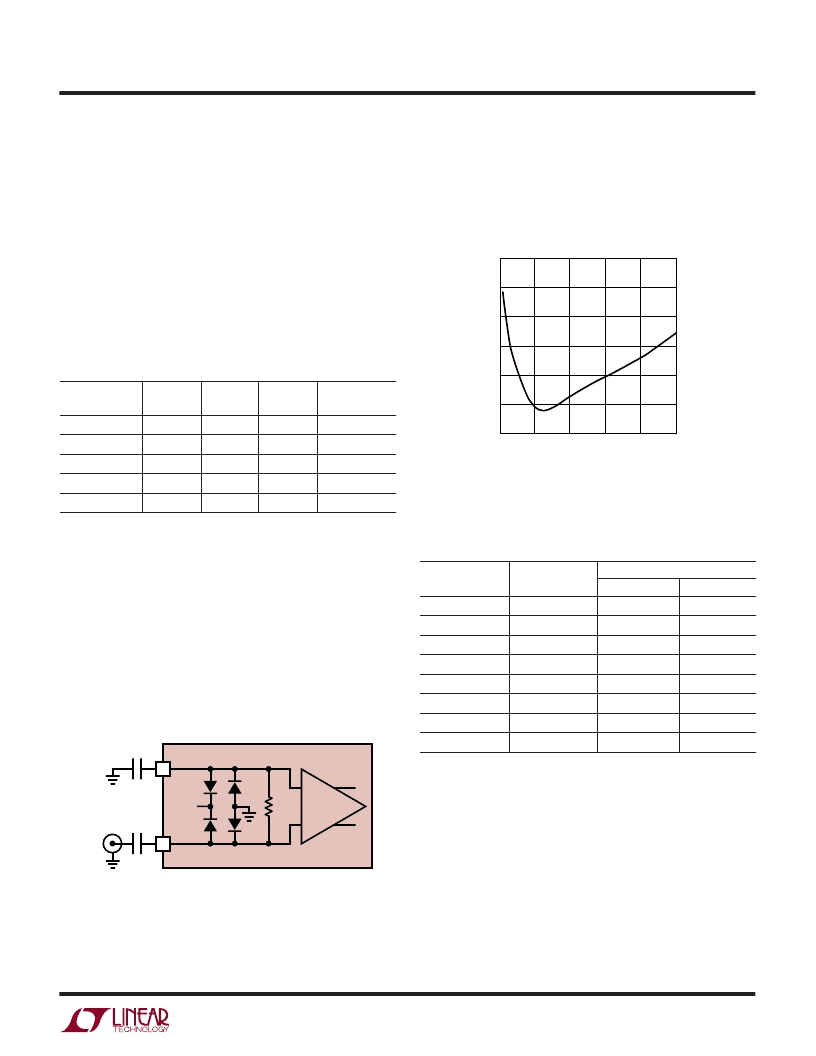
LO Input Port
The LO buffer amplifier consists of high speed limiting
differential amplifiers designed to drive the mixer core for
high linearity. The LO
+
and LO
–
pins are designed for single-
ended drive, though differential drive can be used if de-
sired. The LO input is internally matched to 50
; however,
external DC blocking capacitors are required because the
LO pins are internally biased to approximately 1.7V DC. A
simplified schematic for the LO input is shown in Figure 7.
APPLICATIU
W
U
U
50
C5
100pF
C6
100pF
LO
IN
50
LT5526
LO
–
LO
+
5526 F07
V
CC
14
15
Figure 7. LO Input Schematic
Figure 8. Typical LO Input Return Loss
with 100pF DC Blocking Capacitors
External 100pF DC blocking capacitors provide a broad-
band match from about 110MHz to 2.7GHz, as shown in
the plot of return loss vs frequency in Figure 8. The LO
input match can be improved at lower frequencies by
increasing the values of C5 and C6.
Table 3. Single-Ended LO Input Impedance
FREQUENCY
(MHz)
IMPEDANCE
400
63.4 – j12.0
600
61.6 – j8.38
800
61.8 – j6.86
1000
62.4 – j7.09
1200
62.8 – j8.32
1400
62.6 – j10.3
1600
61.9 – j12.6
1800
60.5 – j14.4
INPUT REFLECTION COEFFICIENT
MAG
0.158
0.128
0.122
0.127
0.135
0.144
0.154
0.160
ANGLE
–35.8
–31.5
–26.6
–26.1
–28.8
–34.0
–40.3
–46.2
IF Output Port
A simplified schematic of the IF output circuit is shown in
Figure 9. The output pins, IF
+
and IF
–
, are internally
connected to the collectors of the mixer switching transis-
tors. Both pins must be biased at the supply voltage, which
can be applied through the center-tap of a transformer or
FREQUENCY (MHz)
0
–30
R
–25
–20
–15
–10
–5
0
500
1000
1500
2000
5526 F08
2500
相關(guān)PDF資料 |
PDF描述 |
|---|---|
| LT5526EUF | High Linearity, Low Power Downconverting Mixer |
| LT6551 | 3.3V Triple and Quad Video Amplifiers |
| LT6550IMS | 3.3V Triple and Quad Video Amplifiers |
| LT6550 | LCD MOD 24X2 CHAR STN SILVER |
| LT6550CMS | 3.3V Triple and Quad Video Amplifiers |
相關(guān)代理商/技術(shù)參數(shù) |
參數(shù)描述 |
|---|---|
| LT5526EUF | 制造商:Linear Technology 功能描述:Up/Down Conv Mixer 5V 2GHz 16-Pin QFN EP |
| LT5526EUF#PBF | 功能描述:IC MIXER DOWNCONVERTER LP 16QFN RoHS:是 類別:RF/IF 和 RFID >> RF 混頻器 系列:LT5526 產(chǎn)品培訓模塊:Lead (SnPb) Finish for COTS Obsolescence Mitigation Program 標準包裝:100 系列:- RF 型:W-CDMA 頻率:2.11GHz ~ 2.17GHz 混頻器數(shù)目:1 增益:17dB 噪音數(shù)據(jù):2.2dB 次要屬性:- 電流 - 電源:11.7mA 電源電壓:2.7 V ~ 3.3 V 包裝:托盤 封裝/外殼:12-VFQFN 裸露焊盤 供應(yīng)商設(shè)備封裝:12-QFN-EP(3x3) |
| LT5526EUF#TR | 制造商:Linear Technology 功能描述:Up/Down Conv Mixer 5V 2GHz 16-Pin QFN EP T/R |
| LT5526EUF#TRPBF | 功能描述:IC MIXER DOWNCONV LP 16QFN RoHS:是 類別:RF/IF 和 RFID >> RF 混頻器 系列:LT5526 產(chǎn)品培訓模塊:Lead (SnPb) Finish for COTS Obsolescence Mitigation Program 標準包裝:100 系列:- RF 型:W-CDMA 頻率:2.11GHz ~ 2.17GHz 混頻器數(shù)目:1 增益:17dB 噪音數(shù)據(jù):2.2dB 次要屬性:- 電流 - 電源:11.7mA 電源電壓:2.7 V ~ 3.3 V 包裝:托盤 封裝/外殼:12-VFQFN 裸露焊盤 供應(yīng)商設(shè)備封裝:12-QFN-EP(3x3) |
| LT5526EUFPBF | 制造商:Linear Technology 功能描述:Downconverter Mixer,LT5526 2GHz QFN |
發(fā)布緊急采購,3分鐘左右您將得到回復。