- 您現(xiàn)在的位置:買賣IC網(wǎng) > PDF目錄383289 > LT5528 (Linear Technology Corporation) 400MHz to 3.7GHz High Signal Level Downconverting Mixer PDF資料下載
參數(shù)資料
| 型號: | LT5528 |
| 廠商: | Linear Technology Corporation |
| 英文描述: | 400MHz to 3.7GHz High Signal Level Downconverting Mixer |
| 中文描述: | 400MHz至3.7GHz高信號電平下變頻混頻器 |
| 文件頁數(shù): | 7/16頁 |
| 文件大?。?/td> | 221K |
| 代理商: | LT5528 |
7
LT5527
5527f
PIU
NC
(Pins 1, 2, 4, 8, 13, 14, 16):
Not Connected Internally.
These pins should be grounded on the circuit board for
improved LO-to-RF and LO-to-IF isolation.
RF (Pin 3):
Single-Ended Input for the RF Signal. This pin
is internally connected to the primary side of the RF input
transformer, which has low DC resistance to ground.
If the
RF source is not DC blocked, then a series blocking
capacitor must be used
. The RF input is internally matched
from 1.7GHz to 3GHz. Operation down to 400MHz or up to
3700MHz is possible with simple external matching.
EN
(Pin 5):
Enable Pin. When the input enable voltage is
higher than 3V, the mixer circuits supplied through Pins 6,
7, 10 and 11 are enabled. When the input voltage is less
than 0.3V, all circuits are disabled. Typical input current is
50
μ
A for EN = 5V and 0
μ
A when EN = 0V. The EN pin should
not be left floating. Under no conditions should the EN pin
voltage exceed V
CC
+ 0.3V, even at start-up.
V
CC2
(Pin 6):
Power Supply Pin for the Bias Circuits.
Typical current consumption is 2.8mA. This pin should be
externally connected to the V
CC1
pin and decoupled with
1000pF and 1
μ
F capacitors.
V
CC1
(Pin 7):
Power Supply Pin for the LO Buffer Circuits.
Typical current consumption is 23.2mA. This pin should
be externally connected to the V
CC2
pin and decoupled
with 1000pF and 1
μ
F capacitors.
GND (Pins 9, 12):
Ground. These pins are internally
connected to the backside ground for improved isolation.
They should be connected to the RF ground on the circuit
board, although they are not intended to replace the
primary grounding through the backside contact of the
package.
IF
–
, IF
+
(Pins 10, 11):
Differential Outputs for the IF
Signal. An impedance transformation may be required to
match the outputs. These pins must be connected to V
CC
through impedance matching inductors, RF chokes or a
transformer center tap.
LO (Pin 15):
Single-Ended Input for the Local Oscillator
Signal. This pin is internally connected to the primary side
of the LO transformer, which is internally DC blocked. An
external blocking capacitor is not required. The LO input is
internally matched from 1.2GHz to 5GHz. Operation down
to 380MHz is possible with simple external matching.
Exposed Pad (Pin 17):
Circuit Ground Return for the
Entire IC. This must be soldered to the printed circuit board
ground plane.
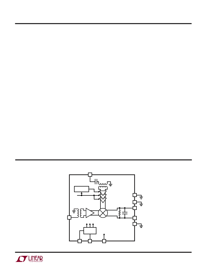
BLOCK DIAGRA
15
7
11
3
6
5
10
DOUBLE-BALANCED
MIXER
LINEAR
AMPLIFIER
LIMITING
AMPLIFIERS
LO
V
CC2
V
CC1
EN
IF
+
12
GND
17
EXPOSED
PAD
IF
–
9
GND
5525 BD
BIAS
RF
V
CC1
REGULATOR
相關(guān)PDF資料 |
PDF描述 |
|---|---|
| LT5526 | High Linearity, Low Power Downconverting Mixer |
| LT5526EUF | High Linearity, Low Power Downconverting Mixer |
| LT6551 | 3.3V Triple and Quad Video Amplifiers |
| LT6550IMS | 3.3V Triple and Quad Video Amplifiers |
| LT6550 | LCD MOD 24X2 CHAR STN SILVER |
相關(guān)代理商/技術(shù)參數(shù) |
參數(shù)描述 |
|---|---|
| LT5528EUF | 制造商:Linear Technology 功能描述:Quadrature Mod 400MHz 16-Pin QFN EP |
| LT5528EUF#PBF | 制造商:Linear Technology 功能描述:Quadrature Mod 400MHz 16-Pin QFN EP 制造商:Linear Technology 功能描述:DEMOD QUADRATURE 1.5-2.4GHZ SMD |
| LT5528EUF#TRPBF | 功能描述:IC QUADRATURE MODULATOR 16-QFN RoHS:是 類別:RF/IF 和 RFID >> RF 調(diào)制器 系列:- 產(chǎn)品培訓(xùn)模塊:Lead (SnPb) Finish for COTS Obsolescence Mitigation Program 標(biāo)準(zhǔn)包裝:2,500 系列:- 功能:調(diào)制器 LO 頻率:700MHz ~ 2.3GHz RF 頻率:700MHz ~ 2.3GHz P1dB:1dBm 底噪:-148dBm/Hz 輸出功率:-1dBm 電流 - 電源:46mA 電源電壓:2.7 V ~ 3.6 V 測試頻率:1.75GHz 封裝/外殼:28-WFQFN 裸露焊盤 包裝:帶卷 (TR) |
| LT5534 | 制造商:LINER 制造商全稱:Linear Technology 功能描述:800MHz to 2.7GHz High Linearity Direct Conversion Quadrature Demodulator |
| LT5534ESC6 | 制造商:Linear Technology 功能描述:RF Power Detector 6-Pin SC-70 |
發(fā)布緊急采購,3分鐘左右您將得到回復(fù)。