- 您現(xiàn)在的位置:買賣IC網(wǎng) > PDF目錄377727 > LTAEZ (Linear Integrated Systems) Differential Input 16-Bit No Latency DS ADC PDF資料下載
參數(shù)資料
| 型號: | LTAEZ |
| 廠商: | Linear Integrated Systems |
| 英文描述: | Differential Input 16-Bit No Latency DS ADC |
| 中文描述: | 差分輸入16位ADC的無延遲局副局長 |
| 文件頁數(shù): | 18/28頁 |
| 文件大小: | 298K |
| 代理商: | LTAEZ |
第1頁第2頁第3頁第4頁第5頁第6頁第7頁第8頁第9頁第10頁第11頁第12頁第13頁第14頁第15頁第16頁第17頁當前第18頁第19頁第20頁第21頁第22頁第23頁第24頁第25頁第26頁第27頁第28頁
LTC2433-1
18
24331fa
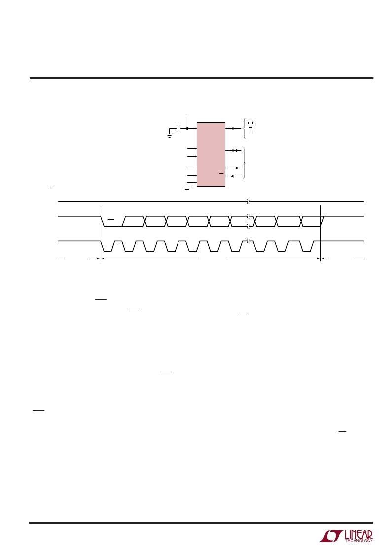
During the conversion, the SCK and the serial data output
pin (SDO) are HIGH (EOC = 1). Once the conversion is
complete, SCK and SDO go LOW (EOC = 0) indicating the
conversion has finished and the device has entered the
data output state. The data output cycle begins on the
first rising edge of SCK and ends after the
19th
rising
edge. Data is shifted out the SDO pin on each falling edge
of SCK. The internally generated serial clock is output
to the SCK pin. This signal may be used to shift the
conversion result into external circuitry. EOC can be
latched on the first rising edge of SCK and the last bit of
the conversion result can be latched on the
19th
rising
edge of SCK. After the
19th
rising edge, SDO goes HIGH
(EOC = 1) indicating a new conversion is in progress. SCK
remains HIGH during the conversion.
PRESERVING THE CONVERTER ACCURACY
The LTC2433-1 is designed to reduce as much as possible
the conversion result sensitivity to device decoupling,
PCB layout, antialiasing circuits, line frequency perturba-
tions and so on. Nevertheless, in order to preserve the
accuracy capability of this part, some simple precautions
are desirable.
Digital Signal Levels
The LTC2433-1’s digital interface is easy to use. Its digital
inputs (F
O
, CS and SCK in External SCK mode of operation)
accept standard TTL/CMOS logic levels and the internal
hysteresis receivers can tolerate edge rates as slow as
100
μ
s. However, some considerations are required to take
advantage of the exceptional accuracy and low supply
current of this converter.
The digital output signals (SDO and SCK in Internal SCK
mode of operation) are less of a concern because they are
not generally active during the conversion state.
While a digital input signal is in the range 0.5V to
(V
CC
–0.5V), the CMOS input receiver draws additional
current from the power supply. It should be noted that,
when any one of the digital input signals (F
O
, CS and SCK
in External SCK mode of operation) is within this range, the
LTC2433-1 power supply current may increase even if the
signal in question is at a valid logic level. For micropower
operation, it is recommended to drive all digital input
signals to full CMOS levels [V
IL
< 0.4V and V
OH
>
(V
CC
– 0.4V)].
Figure 11. Internal Serial Clock, Continuous Operation
SDO
SCK
(INTERNAL)
CS
LSB
MSB
SIG
“O”
BIT 2
BIT 1
BIT 0
BIT 14
BIT 13
BIT 15
BIT 16
BIT 17
EOC
BIT 18
DATA OUTPUT
CONVERSION
CONVERSION
24331 F11
= EXTERNAL CLOCK SOURCE
= INTERNAL OSC/SIMULTANEOUS
50Hz/60Hz REJECTION
V
CC
F
O
REF
+
REF
–
SCK
IN
+
IN
–
GND
SDO
CS
1
10
2
3
9
4
5
6
8
7
REFERENCE
VOLTAGE
0.1V TO V
CC
ANALOG INPUT RANGE
–0.5V
REF
TO 0.5V
REF
1
μ
F
2.7V TO 5.5V
LTC2433-1
3-WIRE
SPI INTERFACE
APPLICATIOU
W
U
U
相關PDF資料 |
PDF描述 |
|---|---|
| LTC2433-1 | Differential Input 16-Bit No Latency DS ADC |
| LTC2433-1CMS | Differential Input 16-Bit No Latency DS ADC |
| LTC2433-1IMS | Differential Input 16-Bit No Latency DS ADC |
| LTC1043CS | Dual Precision Intrumentation Switched-Capacitor Building Block |
| LTC1043CN | Dual Precision Intrumentation Switched-Capacitor Building Block |
相關代理商/技術(shù)參數(shù) |
參數(shù)描述 |
|---|---|
| LTAGL | 制造商:LINER 制造商全稱:Linear Technology 功能描述:100mA, Low Voltage, Very Low Dropout Linear Regulator |
| LT-ALTO350-C | 制造商:LED TEAM 功能描述:DRIVER 3CH DMX FOR RGB LED 350MA |
| LT-ALTO700-C | 制造商:LED TEAM 功能描述:LED DRIVER DC-DC CC 0.7A 制造商:LED TEAM 功能描述:LED DRIVER, DC-DC, CC, 0.7A 制造商:LED TEAM 功能描述:LED DRIVER, DC-DC, CC, 0.7A, Product Range:LED TEAM - ALTO700 Series, Input Volt 制造商:LED TEAM 功能描述:LED DRIVER, DC-DC, CC, 0.7A, Product Range:LED TEAM - ALTO700 Series, Input Voltage Min:24V, Input Voltage Max:32V, Output Current:700mA, Output Power Max:45W, DC / DC Converter Mounting:Panel, Dimming Control Type:PWM, Depth:22mm, , RoHS Compliant: Yes |
| LTALX | 制造商:Apex Tool Group 功能描述:TIP,BENT CHISEL,30 DEG,1.6MM,WP80 |
| L-TAPC64013BLLK3E-DB | 制造商:LSI Corporation 功能描述:HUGHES NETWORK KEY CUSTOMER |
發(fā)布緊急采購,3分鐘左右您將得到回復。