- 您現(xiàn)在的位置:買賣IC網(wǎng) > PDF目錄377733 > LTC1148-3.3 (Linear Technology Corporation) 500kHz and 1MHz High Efficiency 1.5A Switching Regulators; Package: SO; No of Pins: 8; Temperature Range: -40?°C to 85?°C PDF資料下載
參數(shù)資料
| 型號: | LTC1148-3.3 |
| 廠商: | Linear Technology Corporation |
| 元件分類: | 基準(zhǔn)電壓源/電流源 |
| 英文描述: | 500kHz and 1MHz High Efficiency 1.5A Switching Regulators; Package: SO; No of Pins: 8; Temperature Range: -40?°C to 85?°C |
| 中文描述: | 射頻放大器 |
| 文件頁數(shù): | 15/20頁 |
| 文件大小: | 319K |
| 代理商: | LTC1148-3.3 |
15
LTC1148
LTC1148-3.3/LTC1148-5
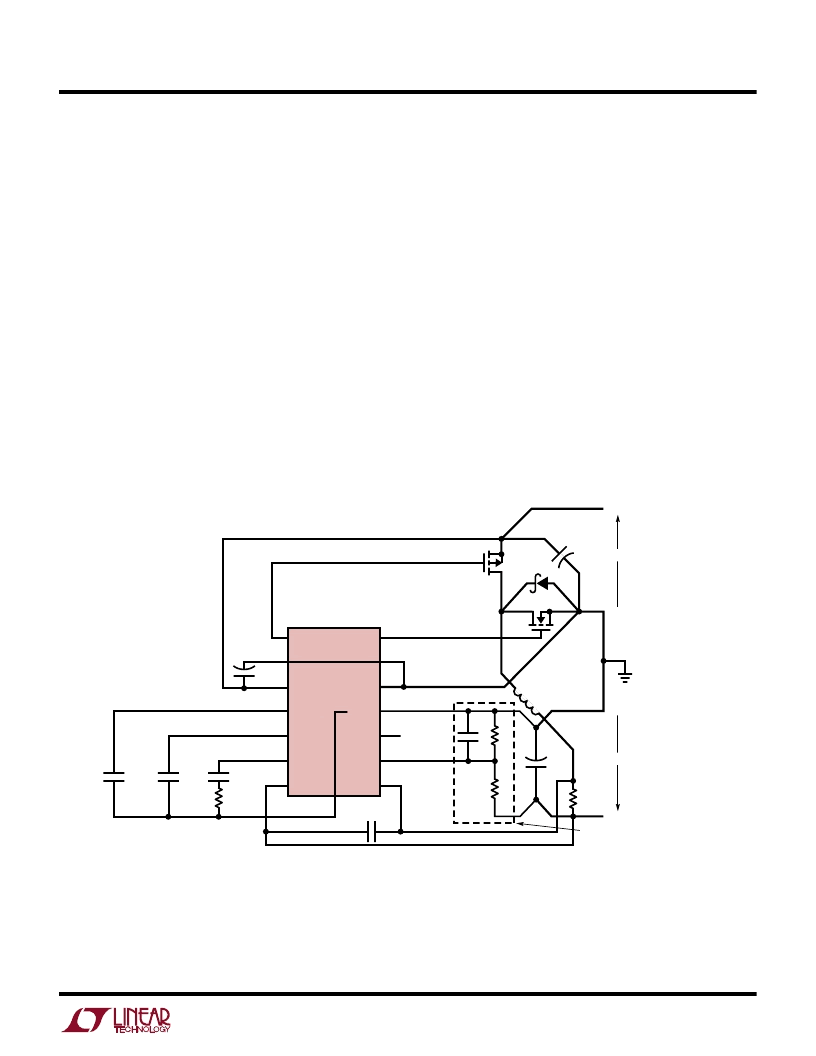
Board Layout Checklist
When laying out the printed circuit board, the following
checklist should be used to ensure proper operation of the
LTC1148 series. These items are also illustrated graphi-
cally in the layout diagram of Figure 9. Check the following
in your layout:
1. Are the signal and power grounds segregated The
LTC1148 signal ground Pin 11 must return to the (–)
plate
of C
OUT
. The power ground returns to the
source of the N-channel MOSFET, anode of the
Schottky diode, and (–) plate of C
IN
, which should
have as short lead lengths as possible.
2. Does the LTC1148 SENSE
–
Pin 7 connect to a point
close to R
SENSE
and the (+) plate of C
OUT
In adjust-
able applications, the resistive divider R1, R2 must be
connected between the (+) plate of C
OUT
and signal
ground.
3. Are the SENSE
–
and SENSE
+
leads routed together
with minimum PC trace spacing The 1000pF capacitor
between Pins 7 and 8 should be as close as possible to
the LTC1148.
4. Does the (+) plate of C
IN
connect to the source of the
P-channel MOSFET as closely as possible This capaci-
tor provides the AC current to the P-channel MOSFET.
5. Is the 1
μ
F V
IN
decoupling capacitor connected closely
between Pin 3 and power ground Pin 12 This capacitor
carries the MOSFET driver peak currents.
6. Is the Shutdown Pin 10 actively pulled to ground during
normal operation The Shutdown pin is high imped-
ance and must not be allowed to float.
Figure 9. LTC1148 Layout Diagram (See Board Layout Checklist)
APPLICATIU
W
U
U
1
2
3
4
5
6
7
14
13
12
11
10
9
8
C
OUT
1
μ
F
D1
P-CHANNEL
1k
3300pF
10nF
C
T
LTC1148
R1
R2
+
R
SENSE
N-CHANNEL
+
C
IN
L
+
–
–
+
V
OUT
V
IN
OUTPUT DIVIDER REQUIRED WITH
ADJUSTABLE VERSION ONLY
BOLD LINES INDICATE HIGH CURRENT PATHS
LTC1148 F09
SHUTDOWN
1000pF
P-DRIVE
V
IN
C
T
INTV
CC
I
TH
SENSE
–
N-DRIVE
PGND
SGND
SHDN
NC (V
FB
)
SENSE
+
NC
NC
+
相關(guān)PDF資料 |
PDF描述 |
|---|---|
| LTC1148-5 | RADIATION HARDENED HIGH EFFICIENCY, 5 AMP SWITCHING REGULATORS |
| LTC1148CN-3.3 | CB 3C 3#16S SKT RECP WALL |
| LTC1148CN-5 | ER 3C 3#16S SKT RECP WALL |
| LTC1148CS-3.3 | RADIATION HARDENED HIGH EFFICIENCY, 5 AMP SWITCHING REGULATORS |
| LTC1148CS-5 | RADIATION HARDENED HIGH EFFICIENCY, 5 AMP SWITCHING REGULATORS |
相關(guān)代理商/技術(shù)參數(shù) |
參數(shù)描述 |
|---|---|
| LTC1148-5 | 制造商:LINER 制造商全稱:Linear Technology 功能描述:High Efficiency Synchronous Step-Down Switching Regulators |
| LTC1148CN | 功能描述:IC REG CTRLR BUCK PWM CM 14-DIP RoHS:否 類別:集成電路 (IC) >> PMIC - 穩(wěn)壓器 - DC DC 切換控制器 系列:- 標(biāo)準(zhǔn)包裝:4,500 系列:PowerWise® PWM 型:控制器 輸出數(shù):1 頻率 - 最大:1MHz 占空比:95% 電源電壓:2.8 V ~ 5.5 V 降壓:是 升壓:無 回掃:無 反相:無 倍增器:無 除法器:無 Cuk:無 隔離:無 工作溫度:-40°C ~ 125°C 封裝/外殼:6-WDFN 裸露焊盤 包裝:帶卷 (TR) 配用:LM1771EVAL-ND - BOARD EVALUATION LM1771 其它名稱:LM1771SSDX |
| LTC1148CN#PBF | 功能描述:IC REG CTRLR BUCK PWM CM 14-DIP RoHS:是 類別:集成電路 (IC) >> PMIC - 穩(wěn)壓器 - DC DC 切換控制器 系列:- 標(biāo)準(zhǔn)包裝:4,500 系列:PowerWise® PWM 型:控制器 輸出數(shù):1 頻率 - 最大:1MHz 占空比:95% 電源電壓:2.8 V ~ 5.5 V 降壓:是 升壓:無 回掃:無 反相:無 倍增器:無 除法器:無 Cuk:無 隔離:無 工作溫度:-40°C ~ 125°C 封裝/外殼:6-WDFN 裸露焊盤 包裝:帶卷 (TR) 配用:LM1771EVAL-ND - BOARD EVALUATION LM1771 其它名稱:LM1771SSDX |
| LTC1148CN-3.3 | 功能描述:IC REG CTRLR BUCK PWM CM 14-DIP RoHS:否 類別:集成電路 (IC) >> PMIC - 穩(wěn)壓器 - DC DC 切換控制器 系列:- 標(biāo)準(zhǔn)包裝:2,500 系列:- PWM 型:電流模式 輸出數(shù):1 頻率 - 最大:500kHz 占空比:96% 電源電壓:4 V ~ 36 V 降壓:無 升壓:是 回掃:無 反相:無 倍增器:無 除法器:無 Cuk:無 隔離:無 工作溫度:-40°C ~ 125°C 封裝/外殼:24-WQFN 裸露焊盤 包裝:帶卷 (TR) |
| LTC1148CN-3.3#PBF | 功能描述:IC REG CTRLR BUCK PWM CM 14-DIP RoHS:是 類別:集成電路 (IC) >> PMIC - 穩(wěn)壓器 - DC DC 切換控制器 系列:- 標(biāo)準(zhǔn)包裝:4,000 系列:- PWM 型:電壓模式 輸出數(shù):1 頻率 - 最大:1.5MHz 占空比:66.7% 電源電壓:4.75 V ~ 5.25 V 降壓:是 升壓:無 回掃:無 反相:無 倍增器:無 除法器:無 Cuk:無 隔離:無 工作溫度:-40°C ~ 85°C 封裝/外殼:40-VFQFN 裸露焊盤 包裝:帶卷 (TR) |
發(fā)布緊急采購,3分鐘左右您將得到回復(fù)。