- 您現(xiàn)在的位置:買賣IC網(wǎng) > PDF目錄224114 > LTC1435IG#TRPBF (LINEAR TECHNOLOGY CORP) High Efficiency Low Noise Synchronous Step-Down Switching Regulator PDF資料下載
參數(shù)資料
| 型號: | LTC1435IG#TRPBF |
| 廠商: | LINEAR TECHNOLOGY CORP |
| 元件分類: | 穩(wěn)壓器 |
| 英文描述: | High Efficiency Low Noise Synchronous Step-Down Switching Regulator |
| 中文描述: | 2 A SWITCHING CONTROLLER, 400 kHz SWITCHING FREQ-MAX, PDSO16 |
| 封裝: | 0.209 INCH, PLASTIC, SSOP-16 |
| 文件頁數(shù): | 3/20頁 |
| 文件大?。?/td> | 338K |
| 代理商: | LTC1435IG#TRPBF |
11
LTC1435
additional circuitry is required to derive INTVCC power
from the output.
The following list summarizes the four possible connec-
tions for EXTVCC:
1. EXTVCC left open (or grounded). This will cause INTVCC
to be powered from the internal 5V regulator resulting
in an efficiency penalty of up to 10% at high input
voltages.
2. EXTVCC connected directly to VOUT. This is the normal
connection for a 5V regulator and provides the highest
efficiency.
3. EXTVCC connected to an output-derived boost network.
For 3.3V and other low voltage regulators, efficiency
gains can still be realized by connecting EXTVCC to an
output-derived voltage which has been boosted to
greater than 4.8V. This can be done with either the
inductive boost winding as shown in Figure 4a or the
capacitive charge pump shown in Figure 4b. The charge
pump has the advantage of simple magnetics.
4. EXTVCC connected to an external supply. If an external
supply is available in the 5V to 10V range (EXTVCC ≤
VIN), it may be used to power EXTVCC providing it is
compatible with the MOSFET gate drive requirements.
When driving standard threshold MOSFETs, the exter-
nal supply must always be present during operation to
prevent MOSFET failure due to insufficient gate drive.
APPLICATIONS INFORMATION
WU
U
INTVCC Regulator
An internal P-channel low dropout regulator produces the
5V supply which powers the drivers and internal circuitry
within the LTC1435. The INTVCC pin can supply up to
15mA and must be bypassed to ground with a minimum
of 2.2
F tantalum or low ESR electrolytic. Good bypassing
is necessary to supply the high transient currents required
by the MOSFET gate drivers.
High input voltage applications, in which large MOSFETs
are being driven at high frequencies, may cause the
maximum junction temperature rating for the LTC1435 to
be exceeded. The IC supply current is dominated by the
gate charge supply current when not using an output
derived EXTVCC source. The gate charge is dependent on
operating frequency as discussed in the Efficiency Consid-
erations section. The junction temperature can be esti-
mated by using the equations given in Note 1 of the
Electrical Characteristics. For example, the LTC1435 is
limited to less than 17mA from a 30V supply:
TJ = 70°C + (17mA)(30V)(100°C/W) = 126°C
To prevent maximum junction temperature from being
exceeded, the input supply current must be checked when
operating in continuous mode at maximum VIN.
EXTVCC Connection
The LTC1435 contains an internal P-channel MOSFET
switch connected between the EXTVCC and INTVCC pins.
The switch closes and supplies the INTVCC power when-
ever the EXTVCC pin is above 4.8V, and remains closed
until EXTVCC drops below 4.5V. This allows the MOSFET
driver and control power to be derived from the output
during normal operation (4.8V < VOUT < 9V) and from the
internal regulator when the output is out of regulation
(start-up, short circuit). Do not apply greater than 10V to
the EXTVCC pin and ensure that EXTVCC < VIN.
Significant efficiency gains can be realized by powering
INTVCC from the output, since the VIN current resulting
from the driver and control currents will be scaled by a
factor of Duty Cycle/Efficiency. For 5V regulators this
supply means connecting the EXTVCC pin directly to VOUT.
However, for 3.3V and other lower voltage regulators,
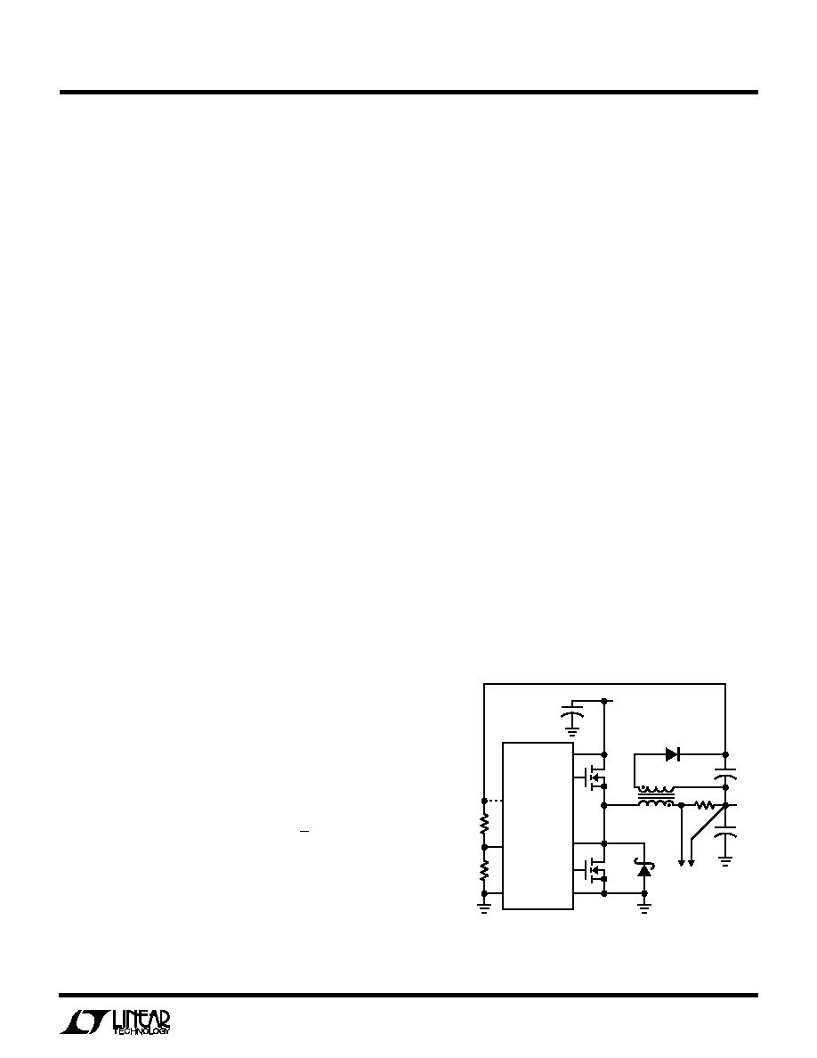
Figure 4a. Secondary Output Loop and EXTVCC Connection
R6
R5
EXTVCC
SFB
SGND
VIN
TG
BG
PGND
LTC1435
N-CH
+
CIN
VIN
1N4148
+
1
F
+
COUT
VSEC
L1
1:N
RSENSE
VOUT
OPTIONAL
EXT VCC
CONNECTION
5V
≤ VSEC ≤ 9V
LTC1435 F04a
SW
相關(guān)PDF資料 |
PDF描述 |
|---|---|
| LTC1436AEGN#PBF | RADIATION HARDENED HIGH EFFICIENCY, 5 AMP SWITCHING REGULATORS |
| LTC2249CUH#TR | 14-Bit, 80Msps Low Power 3V ADC; Package: QFN; No of Pins: 32; Temperature Range: 0°C to +70°C |
| LTC2249IUH#TR | 14-Bit, 80Msps Low Power 3V ADC; Package: QFN; No of Pins: 32; Temperature Range: -40°C to +85°C |
| LTC2250CUH | 10-Bit, 105Msps Low Noise 3V ADCs; Package: QFN; No of Pins: 32; Temperature Range: 0°C to +70°C |
| LTC2250CUH#TR | 10-Bit, 105Msps Low Noise 3V ADCs; Package: QFN; No of Pins: 32; Temperature Range: 0°C to +70°C |
相關(guān)代理商/技術(shù)參數(shù) |
參數(shù)描述 |
|---|---|
| LTC1435IS | 功能描述:IC REG CTRLR BUCK PWM CM 16-SOIC RoHS:否 類別:集成電路 (IC) >> PMIC - 穩(wěn)壓器 - DC DC 切換控制器 系列:- 標準包裝:4,500 系列:PowerWise® PWM 型:控制器 輸出數(shù):1 頻率 - 最大:1MHz 占空比:95% 電源電壓:2.8 V ~ 5.5 V 降壓:是 升壓:無 回掃:無 反相:無 倍增器:無 除法器:無 Cuk:無 隔離:無 工作溫度:-40°C ~ 125°C 封裝/外殼:6-WDFN 裸露焊盤 包裝:帶卷 (TR) 配用:LM1771EVAL-ND - BOARD EVALUATION LM1771 其它名稱:LM1771SSDX |
| LTC1435IS#PBF | 功能描述:IC REG CTRLR BUCK PWM CM 16-SOIC RoHS:是 類別:集成電路 (IC) >> PMIC - 穩(wěn)壓器 - DC DC 切換控制器 系列:- 標準包裝:4,500 系列:PowerWise® PWM 型:控制器 輸出數(shù):1 頻率 - 最大:1MHz 占空比:95% 電源電壓:2.8 V ~ 5.5 V 降壓:是 升壓:無 回掃:無 反相:無 倍增器:無 除法器:無 Cuk:無 隔離:無 工作溫度:-40°C ~ 125°C 封裝/外殼:6-WDFN 裸露焊盤 包裝:帶卷 (TR) 配用:LM1771EVAL-ND - BOARD EVALUATION LM1771 其它名稱:LM1771SSDX |
| LTC1435IS#TR | 制造商:Linear Technology 功能描述:DC DC Cntrlr Single-OUT Sync Step Down 3.5V to 36V Input 16-Pin SOIC N T/R |
| LTC1435IS#TRPBF | 功能描述:IC REG CTRLR BUCK PWM CM 16-SOIC RoHS:是 類別:集成電路 (IC) >> PMIC - 穩(wěn)壓器 - DC DC 切換控制器 系列:- 標準包裝:4,500 系列:PowerWise® PWM 型:控制器 輸出數(shù):1 頻率 - 最大:1MHz 占空比:95% 電源電壓:2.8 V ~ 5.5 V 降壓:是 升壓:無 回掃:無 反相:無 倍增器:無 除法器:無 Cuk:無 隔離:無 工作溫度:-40°C ~ 125°C 封裝/外殼:6-WDFN 裸露焊盤 包裝:帶卷 (TR) 配用:LM1771EVAL-ND - BOARD EVALUATION LM1771 其它名稱:LM1771SSDX |
| LTC1436ACGN | 功能描述:IC REG CTRLR BUCK PWM CM 24-SSOP RoHS:否 類別:集成電路 (IC) >> PMIC - 穩(wěn)壓器 - DC DC 切換控制器 系列:- 標準包裝:4,500 系列:PowerWise® PWM 型:控制器 輸出數(shù):1 頻率 - 最大:1MHz 占空比:95% 電源電壓:2.8 V ~ 5.5 V 降壓:是 升壓:無 回掃:無 反相:無 倍增器:無 除法器:無 Cuk:無 隔離:無 工作溫度:-40°C ~ 125°C 封裝/外殼:6-WDFN 裸露焊盤 包裝:帶卷 (TR) 配用:LM1771EVAL-ND - BOARD EVALUATION LM1771 其它名稱:LM1771SSDX |
發(fā)布緊急采購,3分鐘左右您將得到回復。