- 您現(xiàn)在的位置:買賣IC網(wǎng) > PDF目錄377758 > LTC1628 (Linear Technology Corporation) 500kHz and 1MHz High Efficiency 1.5A Switching Regulators; Package: SO; No of Pins: 8; Temperature Range: -40?°C to 85?°C PDF資料下載
參數(shù)資料
| 型號: | LTC1628 |
| 廠商: | Linear Technology Corporation |
| 元件分類: | 基準電壓源/電流源 |
| 英文描述: | 500kHz and 1MHz High Efficiency 1.5A Switching Regulators; Package: SO; No of Pins: 8; Temperature Range: -40?°C to 85?°C |
| 中文描述: | 射頻放大器 |
| 文件頁數(shù): | 18/32頁 |
| 文件大小: | 366K |
| 代理商: | LTC1628 |
第1頁第2頁第3頁第4頁第5頁第6頁第7頁第8頁第9頁第10頁第11頁第12頁第13頁第14頁第15頁第16頁第17頁當前第18頁第19頁第20頁第21頁第22頁第23頁第24頁第25頁第26頁第27頁第28頁第29頁第30頁第31頁第32頁
18
LTC1628/LTC1628-PG
derived from the output during normal operation (4.7V <
V
OUT
< 7V) and from the internal regulator when the output
is out of regulation (start-up, short-circuit). If more cur-
rent is required through the EXTV
CC
switch than is speci-
fied, an external Schottky diode can be added between the
EXTV
CC
and INTV
CC
pins. Do not apply greater than 7V to
the EXTV
CC
pin and ensure that EXTV
CC
<V
IN
.
Significant efficiency gains can be realized by powering
INTV
CC
from the output, since the V
IN
current resulting
from the driver and control currents will be scaled by a
factor of (Duty Cycle)/(Efficiency). For 5V regulators this
supply means connecting the EXTV
CC
pin directly to V
OUT
.
However, for 3.3V and other lower voltage regulators,
additional circuitry is required to derive INTV
CC
power
from the output.
The following list summarizes the four possible connec-
tions for EXTV
CC:
1. EXTV
CC
Left Open (or Grounded). This will cause INTV
CC
to be powered from the internal 5V regulator resulting in
an efficiency penalty of up to 10% at high input voltages.
2. EXTV
CC
Connected directly to V
OUT
. This is the normal
connection for a 5V regulator and provides the highest
efficiency.
3. EXTV
CC
Connected to an External supply. If an external
supply is available in the 5V to 7V range, it may be used to
power EXTV
CC
providing it is compatible with the MOSFET
gate drive requirements.
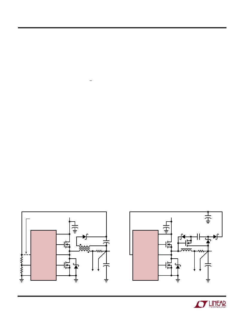
Figure 6a. Secondary Output Loop & EXTV
CC
Connection
Figure 6b. Capacitive Charge Pump for EXTV
CC
4. EXTV
CC
Connected to an Output-Derived Boost Net-
work. For 3.3V and other low voltage regulators, efficiency
gains can still be realized by connecting EXTV
CC
to an
output-derived voltage that has been boosted to greater
than 4.7V. This can be done with either the inductive boost
winding as shown in Figure 6a or the capacitive charge
pump shown in Figure 6b. The charge pump has the
advantage of simple magnetics.
Topside MOSFET Driver Supply (C
B
, D
B
)
External bootstrap capacitors C
B
connected to the BOOST
pins supply the gate drive voltages for the topside MOSFETs.
Capacitor C
B
in the functional diagram is charged though
external diode D
B
from INTV
CC
when the SW pin is low.
When one of the topside MOSFETs is to be turned on, the
driver places the C
B
voltage across the gate-source of the
desired MOSFET. This enhances the MOSFET and turns on
the topside switch. The switch node voltage, SW, rises to
V
IN
and the BOOST pin follows. With the topside MOSFET
on, the boost voltage is above the input supply: V
BOOST
=
V
IN
+ V
INTVCC
. The value of the boost capacitor C
B
needs
to be 100 times that of the total input capacitance of the
topside MOSFET(s). The reverse breakdown of the exter-
nal Schottky diode must be greater than V
IN(MAX)
. When
adjusting the gate drive level, the final arbiter is the total
input current for the regulator. If a change is made and the
input current decreases, then the efficiency has improved.
If there is no change in input current, then there is no
change in efficiency.
EXTV
CC
FCB
SGND
V
IN
TG1
SW
BG1
PGND
LTC1628
R
SENSE
V
OUT
V
SEC
+
C
OUT
+
1
μ
F
1628 F06a
N-CH
N-CH
R6
+
C
IN
V
IN
T1
1:N
OPTIONAL EXTV
CC
CONNECTION
5V < V
SEC
< 7V
R5
EXTV
CC
V
IN
TG1
SW
BG1
PGND
LTC1628
R
SENSE
V
OUT
VN2222LL
+
C
OUT
1628 F06b
N-CH
N-CH
+
C
IN
+
1
μ
F
V
IN
L1
BAT85
BAT85
BAT85
0.22
μ
F
APPLICATIOU
W
U
U
相關PDF資料 |
PDF描述 |
|---|---|
| LTC1629I-PG | RADIATION HARDENED HIGH EFFICIENCY, 5 AMP SWITCHING REGULATORS |
| LTC1629-PG | RADIATION HARDENED HIGH EFFICIENCY, 5 AMP SWITCHING REGULATORS |
| LTC1629CG-PG | RADIATION HARDENED HIGH EFFICIENCY, 5 AMP SWITCHING REGULATORS |
| LTC1629 | Dual LinCMOS(TM) Timer 14-SOIC |
| LTC1629C | Dual LinCMOS(TM) Timer 14-SOIC |
相關代理商/技術(shù)參數(shù) |
參數(shù)描述 |
|---|---|
| LTC1628CG | 功能描述:IC REG CTRLR BUCK PWM CM 28-SSOP RoHS:否 類別:集成電路 (IC) >> PMIC - 穩(wěn)壓器 - DC DC 切換控制器 系列:- 標準包裝:4,500 系列:PowerWise® PWM 型:控制器 輸出數(shù):1 頻率 - 最大:1MHz 占空比:95% 電源電壓:2.8 V ~ 5.5 V 降壓:是 升壓:無 回掃:無 反相:無 倍增器:無 除法器:無 Cuk:無 隔離:無 工作溫度:-40°C ~ 125°C 封裝/外殼:6-WDFN 裸露焊盤 包裝:帶卷 (TR) 配用:LM1771EVAL-ND - BOARD EVALUATION LM1771 其它名稱:LM1771SSDX |
| LTC1628CG#PBF | 功能描述:IC REG CTRLR BUCK PWM CM 28-SSOP RoHS:是 類別:集成電路 (IC) >> PMIC - 穩(wěn)壓器 - DC DC 切換控制器 系列:- 特色產(chǎn)品:LM3753/54 Scalable 2-Phase Synchronous Buck Controllers 標準包裝:1 系列:PowerWise® PWM 型:電壓模式 輸出數(shù):1 頻率 - 最大:1MHz 占空比:81% 電源電壓:4.5 V ~ 18 V 降壓:是 升壓:無 回掃:無 反相:無 倍增器:無 除法器:無 Cuk:無 隔離:無 工作溫度:-5°C ~ 125°C 封裝/外殼:32-WFQFN 裸露焊盤 包裝:Digi-Reel® 產(chǎn)品目錄頁面:1303 (CN2011-ZH PDF) 其它名稱:LM3754SQDKR |
| LTC1628CG#TR | 功能描述:IC REG CTRLR BUCK PWM CM 28-SSOP RoHS:否 類別:集成電路 (IC) >> PMIC - 穩(wěn)壓器 - DC DC 切換控制器 系列:- 標準包裝:4,500 系列:PowerWise® PWM 型:控制器 輸出數(shù):1 頻率 - 最大:1MHz 占空比:95% 電源電壓:2.8 V ~ 5.5 V 降壓:是 升壓:無 回掃:無 反相:無 倍增器:無 除法器:無 Cuk:無 隔離:無 工作溫度:-40°C ~ 125°C 封裝/外殼:6-WDFN 裸露焊盤 包裝:帶卷 (TR) 配用:LM1771EVAL-ND - BOARD EVALUATION LM1771 其它名稱:LM1771SSDX |
| LTC1628CG#TRPBF | 功能描述:IC REG CTRLR BUCK PWM CM 28-SSOP RoHS:是 類別:集成電路 (IC) >> PMIC - 穩(wěn)壓器 - DC DC 切換控制器 系列:- 標準包裝:4,500 系列:PowerWise® PWM 型:控制器 輸出數(shù):1 頻率 - 最大:1MHz 占空比:95% 電源電壓:2.8 V ~ 5.5 V 降壓:是 升壓:無 回掃:無 反相:無 倍增器:無 除法器:無 Cuk:無 隔離:無 工作溫度:-40°C ~ 125°C 封裝/外殼:6-WDFN 裸露焊盤 包裝:帶卷 (TR) 配用:LM1771EVAL-ND - BOARD EVALUATION LM1771 其它名稱:LM1771SSDX |
| LTC1628CGPBF | 制造商:Linear Technology 功能描述:LTC1628 dual SD PS controller |
發(fā)布緊急采購,3分鐘左右您將得到回復。