- 您現(xiàn)在的位置:買賣IC網(wǎng) > PDF目錄385506 > LTC2208IUP-14 (LINEAR TECHNOLOGY CORP) 14-Bit, 130Msps ADC PDF資料下載
參數(shù)資料
| 型號: | LTC2208IUP-14 |
| 廠商: | LINEAR TECHNOLOGY CORP |
| 元件分類: | ADC |
| 英文描述: | 14-Bit, 130Msps ADC |
| 中文描述: | 1-CH 14-BIT PROPRIETARY METHOD ADC, PARALLEL ACCESS, PQCC64 |
| 封裝: | 9 X 9 MM, PLASTIC, MO-220WNJR-5, QFN-64 |
| 文件頁數(shù): | 3/28頁 |
| 文件大小: | 1056K |
| 代理商: | LTC2208IUP-14 |
第1頁第2頁當前第3頁第4頁第5頁第6頁第7頁第8頁第9頁第10頁第11頁第12頁第13頁第14頁第15頁第16頁第17頁第18頁第19頁第20頁第21頁第22頁第23頁第24頁第25頁第26頁第27頁第28頁
LTC2208-14
3
220814f
U
specifications are at T
A
= 25°C. (Note 4)
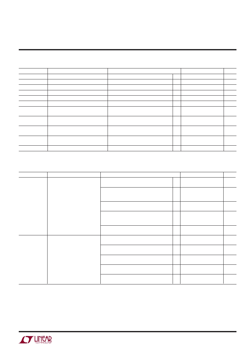
SYMBOL
PARAMETER
V
IN
V
IN, CM
Analog Input Common Mode
I
IN
Analog Input Leakage Current
I
SENSE
SENSE Input Leakage Current
I
MODE
MODE Pin Pull-Down Current to GND
I
LVDS
LVDS Pin Pull-Down Current to GND
C
IN
Analog Input Capacitance
t
AP
Sample-and-Hold
Acquisition Delay Time
t
JITTER
Sample-and-Hold
Acquisition Delay Time Jitter
CMRR
Analog Input
Common Mode Rejection Ratio
BW-3dB
Full Power Bandwidth
U
SYMBOL
SNR
SFDR
PARAMETER
Signal-to-Noise Ratio
Spurious Free
Dynamic Range
2
nd
or 3
rd
Harmonic
CONDITIONS
5MHz Input (2.25V Range, PGA = 0)
5MHz Input (1.5V Range, PGA = 1)
30MHz Input (2.25V Range, PGA = 0) T
A
= 25°C
30MHz Input (2.25V Range, PGA = 0)
30MHz Input (1.5V Range, PGA = 1)
70MHz Input (2.25V Range, PGA = 0)
70MHz Input (1.5V Range, PGA = 1)
140MHz Input (2.25V Range, PGA = 0)
140MHz Input (1.5V Range, PGA = 1) T
A
= 25°C
140MHz Input (1.5V Range, PGA = 1)
250MHz Input (2.25V Range, PGA = 0)
250MHz Input (1.5V Range, PGA =1 )
5MHz Input (2.25V Range, PGA = 0)
5MHz Input (1.5V Range, PGA = 1)
30MHz Input (2.25V Range, PGA = 0)
30MHz Input (1.5V Range, PGA = 1)
70MHz Input (2.25V Range, PGA = 0)
70MHz Input (1.5V Range, PGA = 1)
140MHz Input (2.25V Range, PGA = 0)
140MHz Input (1.5V Range, PGA = 1)
250MHz Input (2.25V Range, PGA = 0)
250MHz Input (1.5V Range, PGA = 1)
MIN
75.7
75.4
73.5
73.3
84
TYP
77.1
74.9
77.0
77.0
74.9
76.9
74.8
76.4
74.6
74.6
75.0
73.6
98
98
96
98
90
93
85
95
76
81
MAX
UNITS
dBFS
dBFS
dBFS
dBFS
dBFS
dBFS
dBFS
dBFS
dBFS
dBFS
dBFS
dBFS
dBc
dBc
dBc
dBc
dBc
dBc
dBc
dBc
dBc
dBc
●
●
●
●
81.5
The
●
denotes the specifications which apply over the full operating temperature range, otherwise
DY
A
IC ACCURACY
U
W
otherwise specifications are at T
A
= 25°C. A
IN
= –1dBFS. (Note 4)
The
●
denotes the specifications which apply over the full operating temperature range,
CONDITIONS
3.135V ≤ V
DD
≤ 3.465V
Differential Input (Note 7)
0V ≤ A
IN+
,
A
IN–
≤ V
DD
0V ≤ SENSE
≤ V
DD
Sample Mode ENC
+
< ENC
–
Hold Mode ENC
+
> ENC
–
MIN
1
–1
–3
TYP
MAX
1.5
1
3
UNITS
V
P-P
Analog Input Range (A
IN+
–
A
IN–
)
1.5 or 2.25
1.25
10
10
6.5
1.8
1.0
●
●
●
V
μA
μA
μA
μA
pF
pF
ns
1V < (A
IN+
= A
IN–
) <1.5V
70
80
fs RMS
dB
R
S
< 25
Ω
700
MHz
相關(guān)PDF資料 |
PDF描述 |
|---|---|
| LTC2208UP-14 | 14-Bit, 130Msps ADC |
| LTC2208 | 16-Bit, 130Msps ADC |
| LTC2208CUP | 16-Bit, 130Msps ADC |
| LTC2208IUP | 16-Bit, 130Msps ADC |
| LTC2208UP | 16-Bit, 130Msps ADC |
相關(guān)代理商/技術(shù)參數(shù) |
參數(shù)描述 |
|---|---|
| LTC2208IUP-14#PBF | 制造商:Linear Technology 功能描述:ADC Single Pipelined 130Msps 14-bit Parallel/LVDS 64-Pin QFN EP 制造商:Linear Technology 功能描述:IC ADC 14BIT 130MSPS 64-QFN |
| LTC2208IUP-14#TR | 制造商:Linear Technology 功能描述:IC ADC 14BIT 130MSPS 64-QFN |
| LTC2208IUP-14#TRPBF | 制造商:Linear Technology 功能描述:ADC Single Pipelined 130Msps 14-bit Parallel/LVDS 64-Pin QFN EP T/R 制造商:Linear Technology 功能描述:IC ADC 14BIT 130MSPS 64-QFN |
| LTC2208IUPPBF | 制造商:Linear Technology 功能描述:ADC, 16 Bit, 130Msps, LTC2208IUPPBF |
| LTC2208UP | 制造商:LINER 制造商全稱:Linear Technology 功能描述:16-Bit, 130Msps ADC |
發(fā)布緊急采購,3分鐘左右您將得到回復(fù)。