- 您現(xiàn)在的位置:買賣IC網(wǎng) > PDF目錄69008 > LTC4558EUD (LINEAR TECHNOLOGY CORP) 1-CHANNEL POWER SUPPLY SUPPORT CKT, PQCC20 PDF資料下載
參數(shù)資料
| 型號: | LTC4558EUD |
| 廠商: | LINEAR TECHNOLOGY CORP |
| 元件分類: | 電源管理 |
| 英文描述: | 1-CHANNEL POWER SUPPLY SUPPORT CKT, PQCC20 |
| 封裝: | 3 X 3 MM, 0.75 MM HEIGHT, PLASTIC, QFN-20 |
| 文件頁數(shù): | 11/12頁 |
| 文件大小: | 146K |
| 代理商: | LTC4558EUD |

LTC4558
8
4558fa
OPERATION
The LTC4558 features two independent SIM/Smart Card
channels. Only one of these channels may be open for
communication at a time however both channels can be
enabled and made ready for communication using the
ENABLEA and ENABLEB pins. This allows faster transi-
tion from one channel to the other. Each channel is able
to produce two voltage levels, 1.8V and 3V. The channel
selection and voltage selection are controlled by the CSEL,
VSELA and VSELB pins as shown in the table below:
Bidirectional Channels
The bidirectional channels are level shifted to the appro-
priate VCCA,B voltages at the I/OA,B pins. An NMOS pass
transistor performs the level shifting. The gate of the NMOS
transistor is biased such that the transistor is completely
off when both sides have relinquished the channel. If one
side of the channel asserts a LOW, then the transistor will
convey the LOW to the other side. Note that current passes
from the receiving side of the channel to the transmitting
side. The low output voltage of the receiving side will be
dependent upon the voltage at the transmitting side plus
the IR drop of the pass transistor.
When a card socket is selected, it becomes a candidate
to drive data on the DATA pin and likewise receive data
from the DATA pin. When a card socket is deselected, its
I/O pin will be pulled HIGH and communication with the
DATA pin will be disabled. If both channels are disabled,
a weak pull-up ensures that the DATA pin is held HIGH,
as long as DVCC is powered.
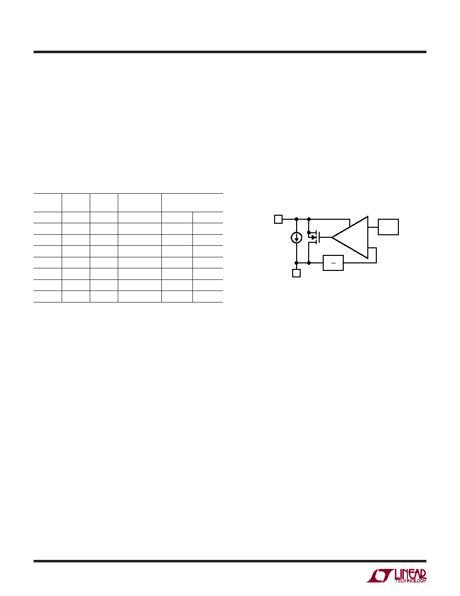
Dynamic Pull-Up Current Sources
The current sources on the bidirectional pins (DATA,I/OA,B)
are dynamically activated to achieve a fast rise time with
a relatively small static current. Once a bidirectional pin
is relinquished, a small start-up current begins to charge
the node. An edge rate detector determines if the pin is
released by comparing its slew rate with an internal refer-
ence value. If a valid transition is detected, a large pull-up
current enhances the edge rate on the node. The higher
slew rate corroborates the decision to charge the node
thereby affecting a dynamic form of hysteresis.
Reset Channels
When a card is selected, the reset channel provides a level
shifted path from the RSTIN pin to the RST pin of the
selected card. When a card is deselected, the last state of
the RSTA,B pin is latched. This allows a deselected card to
remain active, and therefore eliminates delays associated
with card initialization.
Clock Run Mode
Various SIM/Smart Cards may have different requirements
for the state of the clock pin when the channel is not open
for communication. The CLKRUNA,B pins allow the user to
select whether the clock is brought LOW after the channel
is deselected or allowed to run. If a channel is enabled,
bringing its CLKRUN pin HIGH will transmit the clock to
the corresponding card socket, whether or not the channel
is selected using the CSEL.
Figure 1. Dynamic Pull-Up Current Source
Table 1. Channel and Voltage Truth Table
CSEL
VSELA
VSELB
SELECTED
CARD
VOLTAGES
A
B
0
A
1.8V
0
1
A
1.8V
3V
0
1
0
A
3V
1.8V
011
A
3V
1
0
B
1.8V
1
0
1
B
1.8V
3V
1
0
B
3V
1.8V
111
B
3V
VREF
4558 F01
ISTART
BIDIRECTIONAL
PIN
LOCAL
SUPPLY
dv
dt
–
+
相關(guān)PDF資料 |
PDF描述 |
|---|---|
| LTC6405CMS8E#PBF | SPECIALTY ANALOG CIRCUIT, PDSO8 |
| LTC693CS#TRPBF | 1-CHANNEL POWER SUPPLY SUPPORT CKT, PDSO16 |
| LTC692CN8#TRPBF | 1-CHANNEL POWER SUPPLY SUPPORT CKT, PDIP8 |
| LTM4600HVIV#TRPBF | 17 A SWITCHING REGULATOR, BGA104 |
| LTM4600HVEV#TRPBF | 17 A SWITCHING REGULATOR, BGA104 |
相關(guān)代理商/技術(shù)參數(shù) |
參數(shù)描述 |
|---|---|
| LTC4558EUD#PBF | 功能描述:IC SIM/SMART CARD PS 20-QFN RoHS:是 類別:RF/IF 和 RFID >> RF 其它 IC 和模塊 系列:- 標(biāo)準(zhǔn)包裝:100 系列:* |
| LTC4558EUD#TRPBF | 功能描述:IC SIM/SMART CARD PS 20-QFN RoHS:是 類別:RF/IF 和 RFID >> RF 其它 IC 和模塊 系列:- 標(biāo)準(zhǔn)包裝:100 系列:* |
| LTC-4624B | 功能描述:LED 顯示器和配件 Blue 4 Dig 0.4" Ht 466nm 3600ucd RoHS:否 制造商:Avago Technologies 顯示器類型:7 Segment 數(shù)位數(shù)量:2 字符大小:7.8 mm x 14.22 mm 照明顏色:Red 波長:628 nm 共用管腳:Common Anode 工作電壓:2.05 V 工作電流:20 mA 最大工作溫度:+ 85 C 最小工作溫度:- 35 C 封裝:Tube |
| LTC-4624E | 功能描述:LED 顯示器和配件 3 Digit, Orange RoHS:否 制造商:Avago Technologies 顯示器類型:7 Segment 數(shù)位數(shù)量:2 字符大小:7.8 mm x 14.22 mm 照明顏色:Red 波長:628 nm 共用管腳:Common Anode 工作電壓:2.05 V 工作電流:20 mA 最大工作溫度:+ 85 C 最小工作溫度:- 35 C 封裝:Tube |
| LTC-4624G | 功能描述:LED 顯示器和配件 3 Digit, Green RoHS:否 制造商:Avago Technologies 顯示器類型:7 Segment 數(shù)位數(shù)量:2 字符大小:7.8 mm x 14.22 mm 照明顏色:Red 波長:628 nm 共用管腳:Common Anode 工作電壓:2.05 V 工作電流:20 mA 最大工作溫度:+ 85 C 最小工作溫度:- 35 C 封裝:Tube |
發(fā)布緊急采購,3分鐘左右您將得到回復(fù)。