- 您現(xiàn)在的位置:買賣IC網(wǎng) > PDF目錄8611 > LTC6400CUD-26#PBF (Linear Technology)IC ADC DRIVER DIFF 16-QFN PDF資料下載
參數(shù)資料
| 型號: | LTC6400CUD-26#PBF |
| 廠商: | Linear Technology |
| 文件頁數(shù): | 16/16頁 |
| 文件大小: | 0K |
| 描述: | IC ADC DRIVER DIFF 16-QFN |
| 標(biāo)準(zhǔn)包裝: | 121 |
| 類型: | ADC 驅(qū)動器 |
| 應(yīng)用: | 數(shù)據(jù)采集 |
| 安裝類型: | 表面貼裝 |
| 封裝/外殼: | 16-WFQFN 裸露焊盤 |
| 供應(yīng)商設(shè)備封裝: | 16-QFN-EP(3x3) |
| 包裝: | 管件 |

LTC6400-26
9
640026fa
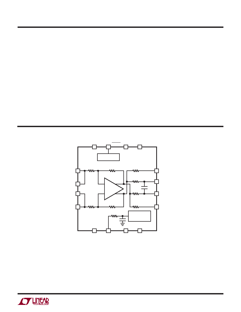
BLOCK DIAGRAM
PIN FUNCTIONS
V+ (Pins 1, 3, 10): Positive Power Supply (Normally tied
to 3V or 3.3V). All three pins must be tied to the same
voltage. Bypass each pin with 1000pF and 0.1μF capaci-
tors as close to the pins as possible.
VOCM (Pin 2): This pin sets the output common mode
voltage. An 0.1μF external bypass capacitor is recom-
mended.
V– (Pins 4, 9, 12, 17):
Negative Power Supply. All four
pins must be connected to same voltage/ground.
–OUT, +OUT (Pins 5, 8): Unltered Outputs. These pins
have series 12.5
Ω resistors ROUT.
–OUTF, +OUTF (Pins 6, 7): Filtered Outputs. These pins
have 50
Ω series resistors and a 2.7pF shunt capacitor.
ENABLE (Pin 11): This pin is a logic input referenced to
VEE. If low, the part is enabled. If high, the part is disabled
and draws very low standby current while the internal op
amp has high output impedance.
+IN (Pins 13, 14): Positive Input. Pins 13 and 14 are
internally shorted together.
–IN (Pins 15, 16): Negative Input. Pins 15 and 16 are
internally shorted together.
Exposed Pad (Pin 17): V–. The Exposed Pad must be
connected to same voltage/ground as pins 4, 9, 12.
13
640026 BD
1
V+
2
VOCM
14
7
15
+OUT
+OUTF
–OUTF
–OUT
+IN
IN+
OUT–
IN–
OUT+
+IN
–IN
5
16
RG
25Ω
ROUT
12.5Ω
RF
500Ω
RG
25Ω
2k
RF
500Ω
6
4
V–
3
V+
12
V–
11
ENABLE
9
V–
10
V+
COMMON
MODE CONTROL
BIAS CONTROL
8
ROUT
12.5Ω
RFILT
50Ω
RFILT
50Ω
CFILT
2.7pF
5.3pF
相關(guān)PDF資料 |
PDF描述 |
|---|---|
| VI-JND-MW-S | CONVERTER MOD DC/DC 85V 100W |
| LTC6360CMS8E#TRPBF | IC ADC DRIVER TRUE ZERO 8MSOP |
| VI-JNB-MW-S | CONVERTER MOD DC/DC 95V 100W |
| VE-B44-MV-B1 | CONVERTER MOD DC/DC 48V 150W |
| SY88843VMG TR | IC AMP POST PECL 3.3V/5V 16-MLF |
相關(guān)代理商/技術(shù)參數(shù) |
參數(shù)描述 |
|---|---|
| LTC6400CUD-26-TRPBF | 制造商:LINER 制造商全稱:Linear Technology 功能描述:1.9GHz Low Noise, Low Distortion Differential ADC Driver for DC-300MHz |
| LTC6400CUD-8 | 制造商:LINER 制造商全稱:Linear Technology 功能描述:2.4GHz Low Noise, Low Distortion Differential ADC |
| LTC6400CUD-8#PBF | 功能描述:IC ADC DRIVER DIFF 2.2GHZ 16QFN RoHS:是 類別:集成電路 (IC) >> 線性 - 放大器 - 專用 系列:- 產(chǎn)品培訓(xùn)模塊:Lead (SnPb) Finish for COTS Obsolescence Mitigation Program 標(biāo)準(zhǔn)包裝:60 系列:- 類型:可變增益放大器 應(yīng)用:CATV 安裝類型:表面貼裝 封裝/外殼:20-WQFN 裸露焊盤 供應(yīng)商設(shè)備封裝:20-TQFN-EP(5x5) 包裝:托盤 |
| LTC6400CUD-8#TR | 制造商:Linear Technology 功能描述:DIFF-AMPLIFIER, 2.2GHZ, QFN-16, No. of Amplifiers:1, Input Offset Voltage:5mV, Gain dB Max:8dB, Bandwidth:2.2GHz, Amplifier Case Style:QFN, No. of Pins:16, Supply Voltage Range:2.85V to 3.5V, Slew Rate:3810V/s, Supply Current:85mA , RoHS Compliant: No |
| LTC6400CUD-8#TRPBF | 功能描述:IC ADC DRIVER DIFF 2.2GHZ 16QFN RoHS:是 類別:集成電路 (IC) >> 線性 - 放大器 - 專用 系列:- 產(chǎn)品培訓(xùn)模塊:Lead (SnPb) Finish for COTS Obsolescence Mitigation Program 標(biāo)準(zhǔn)包裝:60 系列:- 類型:可變增益放大器 應(yīng)用:CATV 安裝類型:表面貼裝 封裝/外殼:20-WQFN 裸露焊盤 供應(yīng)商設(shè)備封裝:20-TQFN-EP(5x5) 包裝:托盤 |
發(fā)布緊急采購,3分鐘左右您將得到回復(fù)。