- 您現(xiàn)在的位置:買賣IC網(wǎng) > PDF目錄367613 > LUCL8560DAU-DT Low-Power SLIC with Ringing PDF資料下載
參數(shù)資料
| 型號: | LUCL8560DAU-DT |
| 英文描述: | Low-Power SLIC with Ringing |
| 中文描述: | 低功耗振鈴用戶接口 |
| 文件頁數(shù): | 40/46頁 |
| 文件大小: | 842K |
| 代理商: | LUCL8560DAU-DT |
第1頁第2頁第3頁第4頁第5頁第6頁第7頁第8頁第9頁第10頁第11頁第12頁第13頁第14頁第15頁第16頁第17頁第18頁第19頁第20頁第21頁第22頁第23頁第24頁第25頁第26頁第27頁第28頁第29頁第30頁第31頁第32頁第33頁第34頁第35頁第36頁第37頁第38頁第39頁當(dāng)前第40頁第41頁第42頁第43頁第44頁第45頁第46頁

40
Lucent Technologies Inc.
Data Sheet
April 2000
L8560 Low-Power SLIC with Ringing
Applications
(continued)
Design Examples
(continued)
Complex Termination Impedance Design Example
Using L8560 Without Spare Op Amp
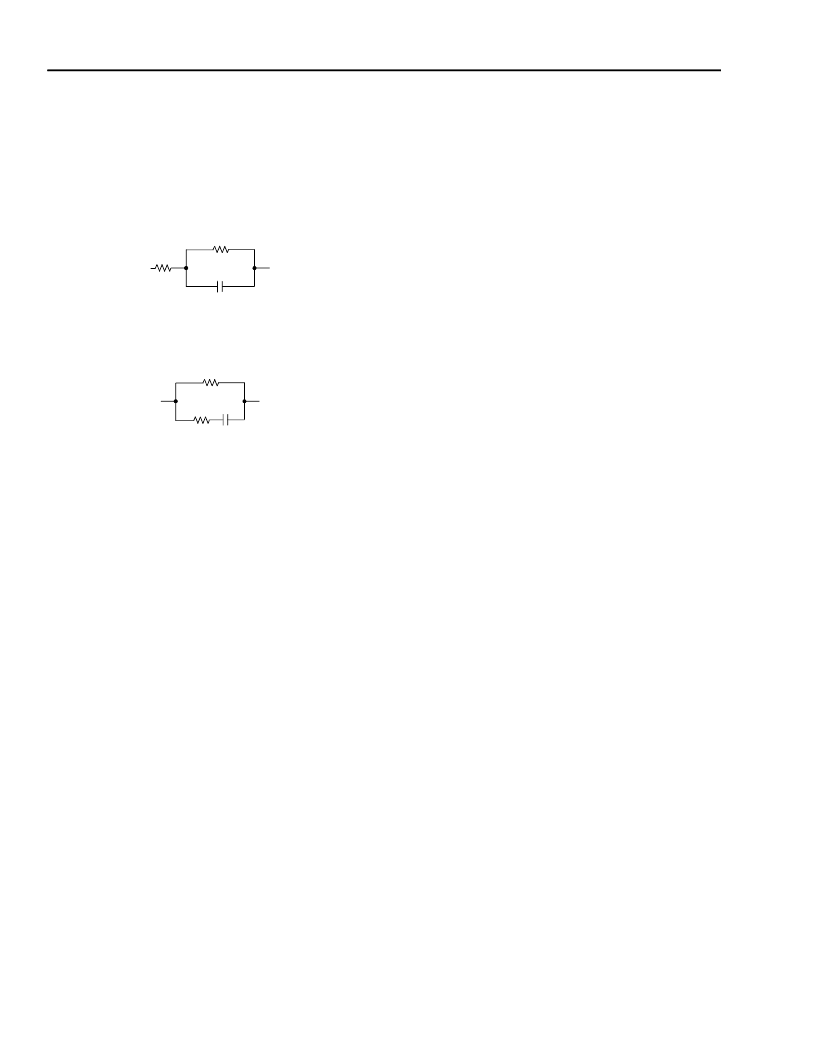
Complex termination is specified in the form:
5-6396(F)
To work with this application, convert termination to the
form:
5-6398(F)
where:
R
1
′ = R
1
+ R
2
1
R
2
R
2
′ =
(R
1
+ R
2
)
C′ =
C
ac Interface Using First-Generation Codec
R
TGP
/R
TGS
/C
GS
(Z
TG
): These components give gain
shaping to get good gain flatness. These components
are a scaled version of the specified complex termina-
tion impedance.
Note for pure (600
) resistive terminations, compo-
nents R
TGS
and C
GS
are not used. Resistor R
TGP
is
used and is still 4.32 k
.
R
X
/R
T6
: With other components set, the transmit gain
(for complex and resistive terminations) R
X
and R
T6
are
varied to give specified transmit gain.
R
T3
/R
RCV
/R
GP
: For both complex and resistive termina-
tions, the ratio of these resistors set the receive gain.
For resistive terminations, the ratio of these resistors
set the return loss characteristic. For complex termina-
tions, the ratio of these resistors set the low-frequency
return loss characteristic.
C
N
/R
N1
/R
N2
: For complex terminations, these compo-
nents provide high-frequency compensation to the
return loss characteristic.
For resistive terminations, these components are not
used and R
CVN
is connected to ground via a resistor.
R
HB
: Sets hybrid balance for all terminations.
Set Z
TG
—gain shaping:
Z
TG
= R
TGP
|| R
TGS
+ C
GS
which is a scaled version of
Z
T/R
(the specified termination resistance) in the
R
1
′ || R
2
′ + C′ form
.
R
TGP
must be 4.32 k
to set SLIC transconductance to
400 V/A
R
TGP
= 4.32 k
At dc,
C
TGS
and C′ are
open.
R
TGP
= M x
R1′
where M is the scale factor.
R
1
′
M =
It can be shown:
R
TGS
= M x
R2′
and
C
TGS
=
R
2
C
R
1
R
1
′
C′
R
2
′
-------
+
R
1
R
2
---------------------
2
--------------
′
M
------
相關(guān)PDF資料 |
PDF描述 |
|---|---|
| LUCL8560FAU-DT | Low-Power SLIC with Ringing |
| LUCL8560DAU-D | Low-Power SLIC with Ringing |
| LUCL8560FAU-D | Low-Power SLIC with Ringing |
| LUCL8560AAU-D | GT 5C 2#0 3#12 SKT RECP WALL |
| LUCL8560AAU-DT | GT 3C 3#0 SKT RECP WALL RM |
相關(guān)代理商/技術(shù)參數(shù) |
參數(shù)描述 |
|---|---|
| LUCL8560EP-D | 制造商:AGERE 制造商全稱:AGERE 功能描述:Low-Power SLIC with Ringing |
| LUCL8560EP-DT | 制造商:AGERE 制造商全稱:AGERE 功能描述:Low-Power SLIC with Ringing |
| LUCL8560FAU-D | 制造商:AGERE 制造商全稱:AGERE 功能描述:Low-Power SLIC with Ringing |
| LUCL8560FAU-DT | 制造商:AGERE 制造商全稱:AGERE 功能描述:Low-Power SLIC with Ringing |
| LUCL8560GP-D | 制造商:AGERE 制造商全稱:AGERE 功能描述:Low-Power SLIC with Ringing |
發(fā)布緊急采購,3分鐘左右您將得到回復(fù)。