- 您現(xiàn)在的位置:買賣IC網(wǎng) > PDF目錄30776 > LV4985V 1.2 W, 2 CHANNEL, AUDIO AMPLIFIER, PDSO14 PDF資料下載
參數(shù)資料
| 型號: | LV4985V |
| 元件分類: | 音頻/視頻放大 |
| 英文描述: | 1.2 W, 2 CHANNEL, AUDIO AMPLIFIER, PDSO14 |
| 封裝: | 0.225 INCH, SSOP-14 |
| 文件頁數(shù): | 14/15頁 |
| 文件大?。?/td> | 401K |
| 代理商: | LV4985V |

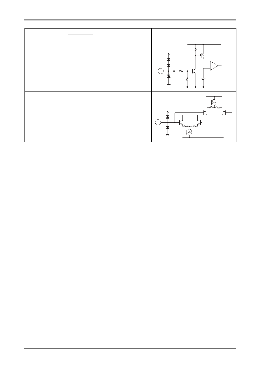
LV4985VH
Continued from preceding page.
Pin Voltage
Pin No.
Pin Name
VCC = 5V
Description
Equivalent Circuit
9
STBY
External apply
Standby/2nd amplifier stop control pin.
0 to 0.3V
Standby mode
1.3 to 1.7V
SE mode
2.3 to VCC BTL mode
+
-
VCC
GND
VB1
150k
Ω
30k
Ω
9
VCC
10
VOL
External apply
Volume control pin.
VCC
GND
10
VCC
Usage Note
1. Input coupling capacitor (C1 and C2)
C1 (C2) is an input coupling capacitor that is used to cut the DC component. The input coupling capacitor C1 (C2) and
the input resisters of 20k
Ω (15kΩ + 5kΩ) make up a high-pass filter, attenuating the bass frequency. Therefore, the
capacitance value must be selected with due consideration of the cut-off frequency.
The cut-off frequencies are expressed by the following formulas.
1ch
fc1 = 1/ (2π × C1 × 20000)
2ch
fc2 = 1/ (2π × C2 × 20000)
This capacitor affects the pop noise at startup. Note with care that increasing the capacitance value lengthens the
charging time of the capacitor, which will make the pop noise louder.
2. Input coupling capacitors (C3 and C4) in the power amplifier block
C3 (C4) is an input coupling capacitor that is used to cut the DC component. The input coupling capacitor C3 (C4) and
the input resistor R1 (R3) make up a high-pass filter, attenuating the bass frequency. Therefore, the capacitance value
must be selected with due consideration of the cut-off frequency.
The cut-off frequencies are expressed by the following formulas.
1ch
fc3 = 1/ (2π × C3 × R1)
2ch
fc4 = 1/ (2π × C4 × R3)
This capacitor affects the pop noise at startup. Note with care that increasing the capacitance value lengthens the
charging time of the capacitor, which will make the pop noise louder.
3. BTL voltage gain of the power amplifier block
The voltage gain of the first amplifier is determined by the ratio between the resistors R1 and R2 (R3 and R4).
1ch
Vg1 = 20 × log (R2/R1) … unit : dB
2ch
Vg2 = 20 × log (R4/R3) … unit : dB
Therefore, the BTL voltage gain of the power amplifier block is expressed by the following formulas.
1ch
VgBTL1 = 6 + 20 × log (R2/R1) … unit : dB
2ch
VgBTL2 = 6 + 20 × log (R4/R3) … unit : dB
The BTL voltage gain of the power amplifier block must be set in the range of 0 to 26dB.
No.A1568-8/15
相關(guān)PDF資料 |
PDF描述 |
|---|---|
| LV4991M | 1 W, 1 CHANNEL, AUDIO AMPLIFIER, PDSO8 |
| LV4991M | 1 W, 1 CHANNEL, AUDIO AMPLIFIER, PDSO8 |
| LV4991TH | 1 W, 1 CHANNEL, AUDIO AMPLIFIER, PDSO8 |
| LV4991TH | 1 W, 1 CHANNEL, AUDIO AMPLIFIER, PDSO8 |
| LV4991TT | 0.45 W, 1 CHANNEL, AUDIO AMPLIFIER, PDSO8 |
相關(guān)代理商/技術(shù)參數(shù) |
參數(shù)描述 |
|---|---|
| LV4985VH | 制造商:SANYO 制造商全稱:Sanyo Semicon Device 功能描述:Bi-CMOS IC For Portable Electronic Device Use 1.2W × 2ch BTL Power Amplifier |
| LV4985VH_0912 | 制造商:SANYO 制造商全稱:Sanyo Semicon Device 功能描述:For Portable Electronic Device Use 1.2W x 2ch BTL Power Amplifier |
| LV4985VH-TLM-H | 功能描述:功率放大器 BTL POWER AMPLIFIER RoHS:否 制造商:TriQuint Semiconductor 封裝 / 箱體: 工作電源電壓:28 V 電源電流:2.5 A 工作溫度范圍: 封裝: |
| LV49-9000 | 制造商:FLOWLINE 功能描述:Sensor Accessory; Cable Hanger |
| LV4991M | 制造商:SANYO 制造商全稱:Sanyo Semicon Device 功能描述:Monaural BTL Power Amplifier |
發(fā)布緊急采購,3分鐘左右您將得到回復(fù)。