- 您現(xiàn)在的位置:買賣IC網(wǎng) > PDF目錄30776 > LV4993M (SANYO SEMICONDUCTOR CO LTD) 1.5 W, 3 CHANNEL, AUDIO AMPLIFIER, PDSO8 PDF資料下載
參數(shù)資料
| 型號: | LV4993M |
| 廠商: | SANYO SEMICONDUCTOR CO LTD |
| 元件分類: | 音頻/視頻放大 |
| 英文描述: | 1.5 W, 3 CHANNEL, AUDIO AMPLIFIER, PDSO8 |
| 封裝: | 0.225 INCH, MFP-8 |
| 文件頁數(shù): | 10/13頁 |
| 文件大小: | 518K |
| 代理商: | LV4993M |

LV4993M
No.A1962-6/13
Cautions for use
1. Input coupling capacitor (C3)
C3 is an input coupling capacitor, and it has aimed at the DC cutting. However, please set it in consideration of the
cutoff frequency when you decide the capacitance value so that the high-pass filter may be composed by this capacitor
(C3) and input resistance (R1), and the bass frequency signal may attenuate.
The cutoff frequency is shown by the next formula.
fc =
1
2π*C3*R1
Moreover, this capacitor influences a pop noise at start-up. Please note it enough so that the charging time to the
capacitor may become long when the value is enlarged, and the pop noise level may grow.
2. BTL voltage gain
The voltage gain of the first amplifier is decided depending on the ratio of resistance R1 and R2.
Vg=20 * log(R2/R1) (dB)
Therefore, the BTL voltage gain:
VgBTL=6+20 * log(R1/R2) (dB)
It is shown by the above-mentioned calculating formula. Please set the BTL voltage gain within the range from 0 to
26dB.
3. Pin 3 capacitor (C4)
C4 is a capacitor for the ripple filter. It is a purpose to compose the low-pass filter of internal resistance
(100k+450k) and C4, to reduce the power supply ripple element, and to improve the ripple elimination factor.
Please operate the automatic pop noise reduction circuit by using the standing up transition response characteristic of
3rd pin voltage (standard voltage), and design in IC in consideration of a pop noise at the time of start-up growing
when the C3 capacity value is reduced to hasten the start-up speed.
4. Capacitor for power supply line (C1, C2)
Bypass capacitor (C2) has aimed at the high frequency aphaeresis that cannot be removed with the power supply
capacitor (C1: Chemical capacitor). This capacity must arrange as much as possible near IC, and use the ceramic
capacitor with good high-frequency property.
It is also possible to bring it together in the ceramic capacitor of one 2.2μF when a steady power supply is used. Please
enlarge the capacity value of power supply capacitor (C1) when the power supply line is comparatively unstable.
5. Standby pin (pin 2)
By controlling the standby pin, the mode changeover can be made between standby and operation modes. The series
resistance (R3:1k or more) is recommended to be inserted might receive the influence of a digital noise from CPU
though it is possible to control with the output port of CPU directly.
Standby mode
V2 = 0 to 0.3V
Operation mode
V2 = 1.6 to 3V
Please suppress the impressed voltage to become a static test mode (heat protection circuit operation check mode)
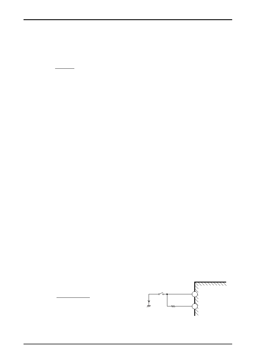
when 3V or more is impressed to 2nd pin within 3V. Moreover, it is also possible to synchronize with the power
supply and to use the pin as shown in Figure 1 when the standby function is not used. Please set the value of series
resistance (R3) so that 2nd pin voltage may become 3V or less.
Current (I2) that flows in 2nd pin can be calculated by the next formula.
I2 =
7*10-6+(VCC0.7)
R3+30000
Fig. 1
VCC
R3
VCC
STBY
7
2
相關PDF資料 |
PDF描述 |
|---|---|
| LV4995TT | 0.25 W, 1 CHANNEL, AUDIO AMPLIFIER, PDSO8 |
| LV51141T | 2-CHANNEL POWER SUPPLY SUPPORT CKT, PDSO6 |
| LV549-CHIP | AUDIO AMPLIFIER, UUC8 |
| LV549-PLID | AUDIO AMPLIFIER, PDSO8 |
| LV549-MCRO | AUDIO AMPLIFIER, PDSO8 |
相關代理商/技術參數(shù) |
參數(shù)描述 |
|---|---|
| LV4993TH | 制造商:SANYO 制造商全稱:Sanyo Semicon Device 功能描述:For Portable Audio Equipment Monaural BTL Power Amplifier |
| LV4R7M2AB-0613(E) | 制造商:SPC Multicomp 功能描述:CAPACITOR 4.7UF 100V |
| LV5012MD-AH | 制造商:ON Semiconductor 功能描述:DIMMABLE LED LIGHTING DRI - Tape and Reel 制造商:ON Semiconductor 功能描述:REEL - DIMMABLE LED LIGHTING DRI |
| LV5017RE6-12N | 功能描述:線性和開關式電源 600W 12V 50A ENCLOSED RoHS:否 制造商:TDK-Lambda 產(chǎn)品:Switching Supplies 開放式框架/封閉式:Enclosed 輸出功率額定值:800 W 輸入電壓:85 VAC to 265 VAC 輸出端數(shù)量:1 輸出電壓(通道 1):20 V 輸出電流(通道 1):40 A 商用/醫(yī)用: 輸出電壓(通道 2): 輸出電流(通道 2): 安裝風格:Rack 長度: 寬度: 高度: |
| LV5017RE6-12NI | 功能描述:線性和開關式電源 600W 12V 50A ENCLOSE FRCD CURRENT SHARING RoHS:否 制造商:TDK-Lambda 產(chǎn)品:Switching Supplies 開放式框架/封閉式:Enclosed 輸出功率額定值:800 W 輸入電壓:85 VAC to 265 VAC 輸出端數(shù)量:1 輸出電壓(通道 1):20 V 輸出電流(通道 1):40 A 商用/醫(yī)用: 輸出電壓(通道 2): 輸出電流(通道 2): 安裝風格:Rack 長度: 寬度: 高度: |
發(fā)布緊急采購,3分鐘左右您將得到回復。