- 您現(xiàn)在的位置:買賣IC網(wǎng) > PDF目錄361046 > LV8572A (National Semiconductor Corporation) LV8572A Low Voltage Real Time Clock (RTC) PDF資料下載
參數(shù)資料
| 型號: | LV8572A |
| 廠商: | National Semiconductor Corporation |
| 英文描述: | LV8572A Low Voltage Real Time Clock (RTC) |
| 中文描述: | LV8572A低電壓實時時鐘(RTC) |
| 文件頁數(shù): | 15/20頁 |
| 文件大?。?/td> | 329K |
| 代理商: | LV8572A |
Functional Description
(Continued)
D7:
This bit is used to program the signal appearing at the
MFO output, as follows:
D7
MFO Output Signal
0
1
Power Fail Interrupt
Buffered Crystal Oscillator
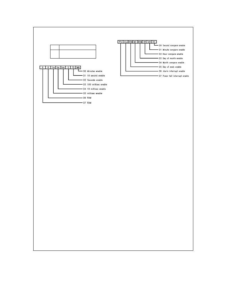
INTERRUPT CONTROL REGISTER 0
TL/F/11417–17
D0–D5:
These bits are used to enable one of the selected
periodic interrupts by writing a one into the appropriate bit.
These interrupts are issued at the rollover of the clock. For
example, the minutes interrupt will be issued whenever the
minutes counter increments. In all likelihood the interrupt
will be enabled asynchronously with the real time change.
Therefore, the very first interrupt will occur in less than the
periodic time chosen, but after the first interrupt all subse-
quent interrupts will be spaced correctly. These interrupts
are useful when minute, second, real time reading, or task
switching is required. When all six bits are written to a 0 this
disables periodic interrupts from the Main Status Register
and the interrupt pin.
D6 and D7:
General Purpose RAM.
INTERRUPT CONTROL REGISTER 1
TL/F/11417–18
D0–D5:
Each of these bits are enable bits which will enable
a comparison between an individual clock counter and its
associated compare RAM. If any bit is a zero then that
clock-RAM comparator is set to the ‘‘a(chǎn)lways equal’’ state
and the associated TIME COMPARE RAM byte can be used
as general purpose RAM. However, to ensure that an alarm
interrupt is not generated at bit D3 of the Main Status Regis-
ter, all bits must be written to a logic zero.
D6:
In order to generate an external alarm compare inter-
rupt to the
m
P from bit D3 of the Main Status Register, this
bit must be written to a logic 1. If battery backed mode is
selected then this bit is controlled by D4 of the Real Time
Mode Register.
D7:
The MSB of this register is the enable bit for the Power
Fail Interrupt. When this bit is set to a one an interrupt will
be generated to the
m
P when V
BB
l
V
CC
. If battery backed
mode is selected then this bit is controlled by D4 of the Real
Time Mode Register.
This bit also enables the low battery detection analog cir-
cuitry.
15
相關(guān)PDF資料 |
PDF描述 |
|---|---|
| LV8572AM | LV8572A Low Voltage Real Time Clock (RTC) |
| LV8572AN | LV8572A Low Voltage Real Time Clock (RTC) |
| LV8573A | LV8573A Low Voltage Real Time Clock (RTC) |
| LV8573AM | LV8573A Low Voltage Real Time Clock (RTC) |
| LV8573AN | LV8573A Low Voltage Real Time Clock (RTC) |
相關(guān)代理商/技術(shù)參數(shù) |
參數(shù)描述 |
|---|---|
| LV8572AM | 制造商:NSC 制造商全稱:National Semiconductor 功能描述:LV8572A Low Voltage Real Time Clock (RTC) |
| LV8572AMX | 制造商:未知廠家 制造商全稱:未知廠家 功能描述:Real-Time Clock |
| LV8572AN | 制造商:Rochester Electronics LLC 功能描述:- Bulk |
| LV8572AVX | 制造商:未知廠家 制造商全稱:未知廠家 功能描述:Real-Time Clock |
| LV8573A | 制造商:NSC 制造商全稱:National Semiconductor 功能描述:LV8573A Low Voltage Real Time Clock (RTC) |
發(fā)布緊急采購,3分鐘左右您將得到回復(fù)。