- 您現(xiàn)在的位置:買賣IC網(wǎng) > PDF目錄358962 > LVXT8051 (ON SEMICONDUCTOR) Analog Multiplexer / Demultiplexer High−Performance Silicon−Gate CMOS PDF資料下載
參數(shù)資料
| 型號(hào): | LVXT8051 |
| 廠商: | ON SEMICONDUCTOR |
| 英文描述: | Analog Multiplexer / Demultiplexer High−Performance Silicon−Gate CMOS |
| 文件頁(yè)數(shù): | 1/12頁(yè) |
| 文件大小: | 172K |
| 代理商: | LVXT8051 |

Semiconductor Components Industries, LLC, 2005
March, 2005 Rev. 3
1
Publication Order Number:
MC74LVXT8051/D
MC74LVXT8051
Analog Multiplexer /
Demultiplexer
HighPerformance SiliconGate CMOS
The MC74LVXT8051 utilizes silicongate CMOS technology to
achieve fast propagation delays, low ON resistances, and low OFF
leakage currents. This analog multiplexer/demultiplexer controls
analog voltages that may vary across the complete power supply range
(from V
CC
to GND).
The LVXT8051 is similar in pinout to the highspeed HC4051A
and the metalgate MC14051B. The ChannelSelect inputs determine
which one of the Analog Inputs/Outputs is to be connected by means
of an analog switch to the Common Output/Input. When the Enable
pin is HIGH, all analog switches are turned off.
The ChannelSelect and Enable inputs are compatible with
TTLtype input thresholds. The input protection circuitry on this
device allows overvoltage tolerance on the input, allowing the device
to be used as a logiclevel translator from 3.0 V CMOS logic to 5.0V
CMOS Logic or from 1.8V CMOS logic to 3.0 V CMOS Logic while
operating at the highervoltage power supply.
The MC74LVXT8051 input structure provides protection when
voltages up to 7.0 V are applied, regardless of the supply voltage. This
allows the MC74LVXT8051 to be used to interface 5.0 V circuits to
3.0 V circuits.
This device has been designed so that the ON resistance (R
on
) is
more linear over input voltage than R
on
of metalgate CMOS analog
switches.
Features
Fast Switching and Propagation Speeds
Low Crosstalk Between Switches
Diode Protection on All Inputs/Outputs
Analog Power Supply Range (V
CC
GND) = 2.0 to 6.0 V
Digital (Control) Power Supply Range (V
CC
GND) = 2.0 to 6.0 V
Improved Linearity and Lower ON Resistance Than MetalGate
Counterparts
Low Noise
In Compliance With the Requirements of JEDEC Standard No. 7A
PbFree Packages are Available*
*For additional information on our PbFree strategy and soldering details, please
download the ON Semiconductor Soldering and Mounting Techniques
Reference Manual, SOLDERRM/D.
http://onsemi.com
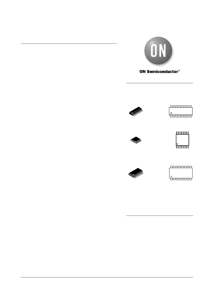
MARKING
DIAGRAMS
A
WL or L
Y
WW or W
=
=
=
=
Assembly Location
Wafer Lot
Year
Work Week
TSSOP16
DT SUFFIX
CASE 948F
SOEIAJ16
M SUFFIX
CASE 966
SOIC16
D SUFFIX
CASE 751B
See detailed ordering and shipping information in the package
dimensions section on page 2 of this data sheet.
ORDERING INFORMATION
LVXT8051
AWLYWW
LVXT
8051
ALYW
LVXT8051
ALYW
1
16
1
16
1
16
相關(guān)PDF資料 |
PDF描述 |
|---|---|
| LVXT8053 | Analog Multiplexer / Demultiplexer High−Performance Silicon−Gate CMOS |
| LW101 | INFRARED LAMP LED |
| LW141 | BLUE OVAL LAMP LED |
| LW160Z | GREEN OVAL LAMP LED |
| LW191 | RED OVAL LAMP LED |
相關(guān)代理商/技術(shù)參數(shù) |
參數(shù)描述 |
|---|---|
| LVXT8053 | 制造商:ONSEMI 制造商全稱:ON Semiconductor 功能描述:Analog Multiplexer / Demultiplexer High−Performance Silicon−Gate CMOS |
| LVXZ161284 WAF | 制造商:Fairchild Semiconductor Corporation 功能描述: |
| LVY12241 | 制造商:LIGITEK 制造商全稱:LIGITEK electronics co., ltd. 功能描述:SUPER BRIGHT ROUND TYPE LED LAMPS |
| LVY12243 | 制造商:LIGITEK 制造商全稱:LIGITEK electronics co., ltd. 功能描述:SUPER BRIGHT ROUND TYPE LED LAMPS |
| LVY12343-PF | 制造商:LIGITEK 制造商全稱:LIGITEK electronics co., ltd. 功能描述:SUPER BRIGHT ROUND TYPE LED LAMPS |
發(fā)布緊急采購(gòu),3分鐘左右您將得到回復(fù)。