- 您現(xiàn)在的位置:買賣IC網(wǎng) > PDF目錄30778 > LX1705ILQ-TR (MICROSEMI CORP-ANALOG MIXED SIGNAL GROUP) 8 W, 2 CHANNEL, AUDIO AMPLIFIER, PQCC32 PDF資料下載
參數(shù)資料
| 型號: | LX1705ILQ-TR |
| 廠商: | MICROSEMI CORP-ANALOG MIXED SIGNAL GROUP |
| 元件分類: | 音頻/視頻放大 |
| 英文描述: | 8 W, 2 CHANNEL, AUDIO AMPLIFIER, PQCC32 |
| 封裝: | 5 X 5 MM, ROHS COMPLIANT, MLPQ-32 |
| 文件頁數(shù): | 3/17頁 |
| 文件大?。?/td> | 378K |
| 代理商: | LX1705ILQ-TR |

LX1705
PRODUCTION DATA SHEET
Microsemi
Analog Mixed Signal Group
11861 Western Avenue, Garden Grove, CA. 92841, 714-898-8121, Fax: 714-893-2570
Page 11
Copyright
2007
Rev. 1.2, 2007-03-20
WWW
.Microse
m
i
.CO
M
8+8W Stereo Filterless Class-D Amplifier
TM
APPLICATION NOTE/PCB D E SI GN GUID E LIN E (CONTINUED )
EXPOSED PAD PCB DESIGN
The construction of the Exposed Pad MLP enables
enhanced thermal and electrical characteristics. In order to
take full advantage of this feature the exposed pad must be
physically connected to the PCB substrate with solder. The
exposed pad is internally connected to the die substrate, so
it is very important that the PCB substrate potential be
connected to the same potential as AVSS.
The PCB thermal pad dimensions should be greater than
the dimensions of the MLPQ thermal pad whenever
possible; however adequate clearance must be met to
prevent solder bridging to the outer pads. A minimum
clearance of 0.2mm is recommended. If this clearance
cannot be met, then the PCB thermal pad should be reduced
in area.
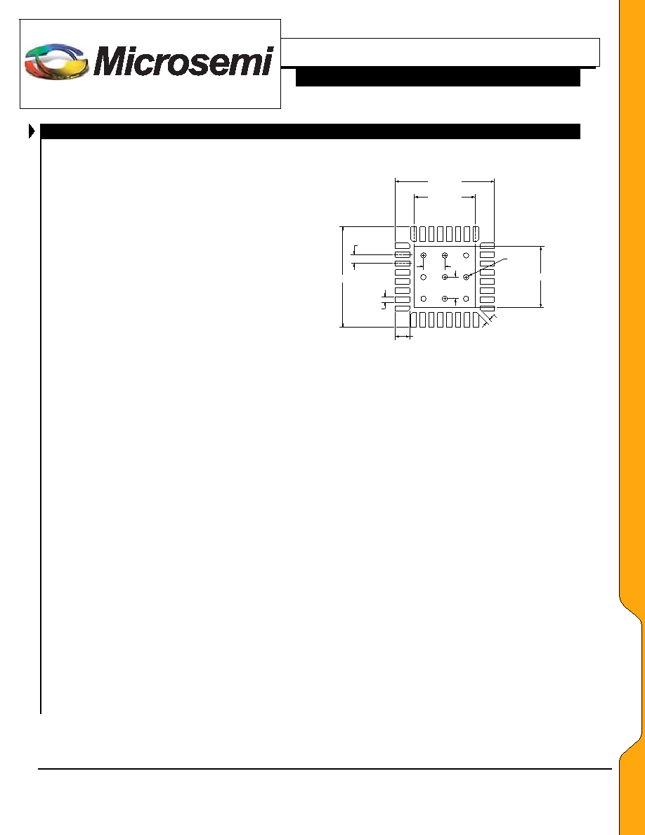
THERMAL PAD VIA DESIGN
There are two types of on-board thermal pad designs:
one using thermal vias to sink the heat to an inner layer
utilizing a copper plane. Based on the JEDEC Specification
(JESD 51-5) the thermal vias should be designed similar to
Figure 5, with the following specifications:
Via Barrel diameter: 0.3mm
Min. Via Barrel plating: 0.025mm
Center to center spacing: 1.2mm
For the LX1705 5x5mm MLPQ package, there will be
enough space for 9 vias. This method is recommended for
use on a multilayer board, and will give the best thermal
performance. Thermal vias may be used on a two layer
board as well, with reduced performance.
Another method is the no via thermal pad, which uses
only the copper pad as a heat sink, and relies on the PCB
substrate material for thermal conduction. This type of
thermal pad is good for a two layer board; however thermal
performance will not be as good as the thermal via method
on a multilayer board.
0.25mm
[0.01
0]
MI
N.
4P
LS
.
0.30mm [0.012]
MAX. 32 PLS.
3.40mm [0.134]
5.56mm [0.219]
0.81mm [0.032]
5.56mm [0.219]
0.50mm [0.020]
TYP. 32 PLS.
1.20mm
[0.047]
6 PLS.
1.20mm
[0.047]
6 PLS.
0.30mm
[0.012]
9 PLS.
Figure 5 – Recommended Land Pad with Vias for 5x5mm
LQ package
AA
PP
LL
IICC
AA
TT
IIOO
NN
SS
相關PDF資料 |
PDF描述 |
|---|---|
| LX1708ILQ-TR | 15 W, 2 CHANNEL, AUDIO AMPLIFIER, PQCC32 |
| LX1720-01CDBT | 2 CHANNEL, AUDIO AMPLIFIER, PDSO44 |
| LX1720-01DB | 2 CHANNEL, AUDIO AMPLIFIER, PDSO44 |
| LX1720-01DB | 2 CHANNEL, AUDIO AMPLIFIER, PDSO44 |
| LX1720-01CDB | 2 CHANNEL, AUDIO AMPLIFIER, PDSO44 |
相關代理商/技術參數(shù) |
參數(shù)描述 |
|---|---|
| LX1708 | 制造商:MICROSEMI 制造商全稱:Microsemi Corporation 功能描述:15+15W Stereo Filterless Class-D Amplifier |
| LX1708 EVAL KIT | 制造商:Microsemi Corporation 功能描述:AUDIOMAX PRODUCTS - Bulk |
| LX1708ILQ | 制造商:Microsemi Corporation 功能描述:AUDIOMAX PRODUCTS - Bulk |
| LX1710 | 制造商:MICROSEMI 制造商全稱:Microsemi Corporation 功能描述:Class-D Mono Power Amplifier Controller IC |
| LX1710-1 | 制造商:MICROSEMI 制造商全稱:Microsemi Corporation 功能描述:EVALUATION KIT |
發(fā)布緊急采購,3分鐘左右您將得到回復。