- 您現(xiàn)在的位置:買賣IC網(wǎng) > PDF目錄30778 > LX1725ILQ (MICROSEMI CORP) 16 W, 2 CHANNEL, AUDIO AMPLIFIER, PQCC32 PDF資料下載
參數(shù)資料
| 型號: | LX1725ILQ |
| 廠商: | MICROSEMI CORP |
| 元件分類: | 音頻/視頻放大 |
| 英文描述: | 16 W, 2 CHANNEL, AUDIO AMPLIFIER, PQCC32 |
| 封裝: | 7 X 7 MM, ROHS COMPLIANT, PLASTIC, MLPQ-32 |
| 文件頁數(shù): | 2/23頁 |
| 文件大?。?/td> | 377K |
| 代理商: | LX1725ILQ |

LX1725
PRODUCTION DATA SHEET
Microsemi
Integrated Products Division
11861 Western Avenue, Garden Grove, CA. 92841, 714-898-8121, Fax: 714-893-2570
10
Page
WWW
.Microse
m
i
.CO
M
15W+15W Stereo Class-D Amplifier
Filterless 30W Mono in BTL
Copyright
2004
Rev. 1.1, 2005-11-04
TM
FUNCTION DESCRIPT ION ( CONTINUED)
STAND BY
Forcing the STBY pin high puts the LX1725 into a zero current
sleep mode. The outputs enter a high impedance mode and all
internal bias circuits are disabled.
OVER CURRENT LIMIT
The LX1725 has built-in over circuit protection. The circuit works
by monitoring the voltage drop across whichever power FET is
active. When this voltage is greater than a certain threshold, an
over-current condition is assumed. If this condition occurs during
five consecutive clock cycles, then the output transistors are
immediately disabled. The hiccup counter then counts 65536 clock
cycles before allowing the outputs to begin switching again.
During this period the FLAG pin goes to HIGH to indicate a
system fault. A “hiccup” condition will be clearly audible if a
speaker is connected to the outputs. The threshold for the over-
current condition is set to 3.75A.
The over current circuit hiccup protection can be disabled by
pulling the RILIM pin to V5V.
UNDER VOLTAGE LOCK-OUT (UVLO)
If the voltage drops below ±5V under dual supply operation or 10V
under single supply operation, the under voltage lock out circuit is
activated and the LX1725 will enter the standby mode. This
switch-off will be silent and without pop noise. It will be recovered
when the supply voltage rises above the threshold level.
The FLAG pin will go logic HIGH to indicate the system fault. A
similar circuit monitors V5V with a threshold of 4V.
THERMAL PROTECTION
When the junction temperature exceeds 125
°C, the gain is reduced
by 6dB (gain fold back) to reduce the output power and on-chip
power dissipation., when the temperature drops below 110
°C the
gain will returns to normal. When the temperature exceeds 155
°C
the outputs are shut off to force the output current to zero. Again,
when the temperature drops below 130
°C the outputs are allowed
to switch and normal operation resumes.
AUDIO INPUT
For a high common mode rejection ratio and a maximum
flexibility in the application, the audio inputs are fully differential.
By connecting the inputs anti-parallel the phase of one of the
channels can be inverted, so that a load can be connected between
the two output filters. In this case the system operates as a mono
BTL amplifier and with the same loudspeaker impedance an
approximately four times higher output power can be obtained.
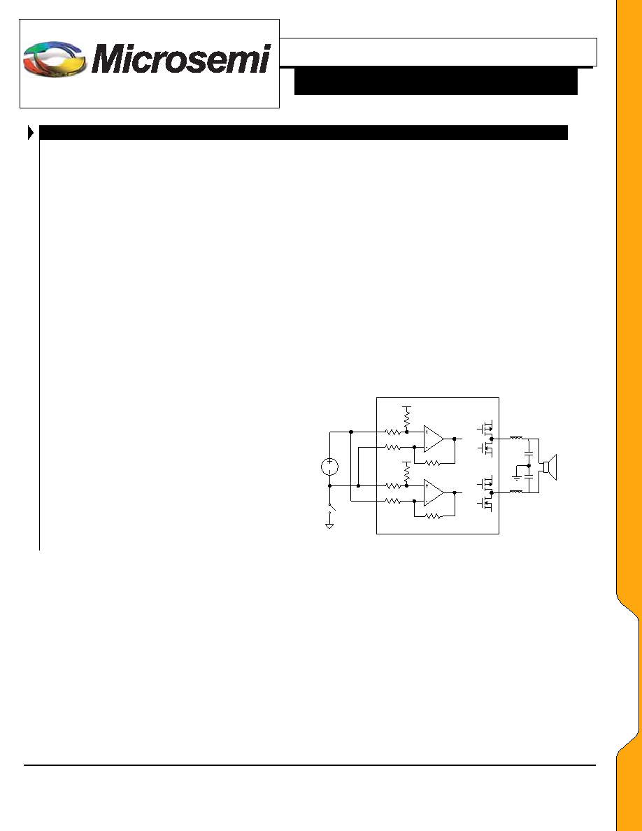
The input configuration for a mono BTL application is illustrated
in Figure 6. In the stereo single-ended configuration it is also
recommended to connect the two differential inputs in anti-phase.
This has advantages for the current handling of the power supply at
low signal frequencies.
Vref
LX1725
IN1+
IN2-
IN2+
IN1-
OUT1
OUT2
Figure 6 – Audio Input Block Diagram
DD
EE
SS
CC
RR
IIPP
TT
IIOO
NN
相關PDF資料 |
PDF描述 |
|---|---|
| LX1790BD | 1 CHANNEL, AUDIO AMPLIFIER, UUC7 |
| LX1790LM | 1 CHANNEL, AUDIO AMPLIFIER, PDSO8 |
| LX1790CJ | 1 CHANNEL, AUDIO AMPLIFIER, CDIP14 |
| LX1790CBD | 1 CHANNEL, AUDIO AMPLIFIER, UUC7 |
| LX1790CLM | 1 CHANNEL, AUDIO AMPLIFIER, PDSO8 |
相關代理商/技術參數(shù) |
參數(shù)描述 |
|---|---|
| LX1725ILQTR | 制造商:Microsemi Corporation 功能描述:Audio Amp Speaker 1-CH Mono/2-CH Stereo 32W Class-D 32-Pin MLPQ T/R |
| LX1725ILQ-TR | 制造商:Microsemi Corporation 功能描述:AUD AMP SPKR 1CH MONO/2CH STEREO 32W/16W CLS-D 32MLPQ - Tape and Reel |
| LX1732 | 制造商:MICROSEMI 制造商全稱:Microsemi Corporation 功能描述:High Current PFM Boost Converter |
| LX1732-03 EVAL KIT | 制造商:Microsemi Corporation 功能描述:DC:DC CONVERTER - Bulk |
| LX1732-05 EVAL KIT | 制造商:Microsemi Corporation 功能描述:DC:DC CONVERTER - Bulk |
發(fā)布緊急采購,3分鐘左右您將得到回復。