- 您現(xiàn)在的位置:買賣IC網(wǎng) > PDF目錄367620 > LX1741CDU (MICROSEMI CORP-ANALOG MIXED SIGNAL GROUP) High Efficiency High Voltage Boost Controller PDF資料下載
參數(shù)資料
| 型號: | LX1741CDU |
| 廠商: | MICROSEMI CORP-ANALOG MIXED SIGNAL GROUP |
| 元件分類: | 穩(wěn)壓器 |
| 英文描述: | High Efficiency High Voltage Boost Controller |
| 中文描述: | 0.145 A SWITCHING CONTROLLER, PDSO8 |
| 封裝: | PLASTIC, MSOP-8 |
| 文件頁數(shù): | 9/15頁 |
| 文件大小: | 459K |
| 代理商: | LX1741CDU |

Microsemi
Integrated Products Division
11861 Western Avenue, Garden Grove, CA. 92841, 714-898-8121, Fax: 714-893-2570
Page 9
Copyright
2000
Rev. 1.1, 2002-11-21
W
M
.
C
LX1741
High Efficiency High Voltage Boost Controller
P
RODUCTION
D
ATA
S
HEET
I N T E G R A T E D P R O D U C T S
E V A L U A T I O N B O A R D
O
VERVIEW
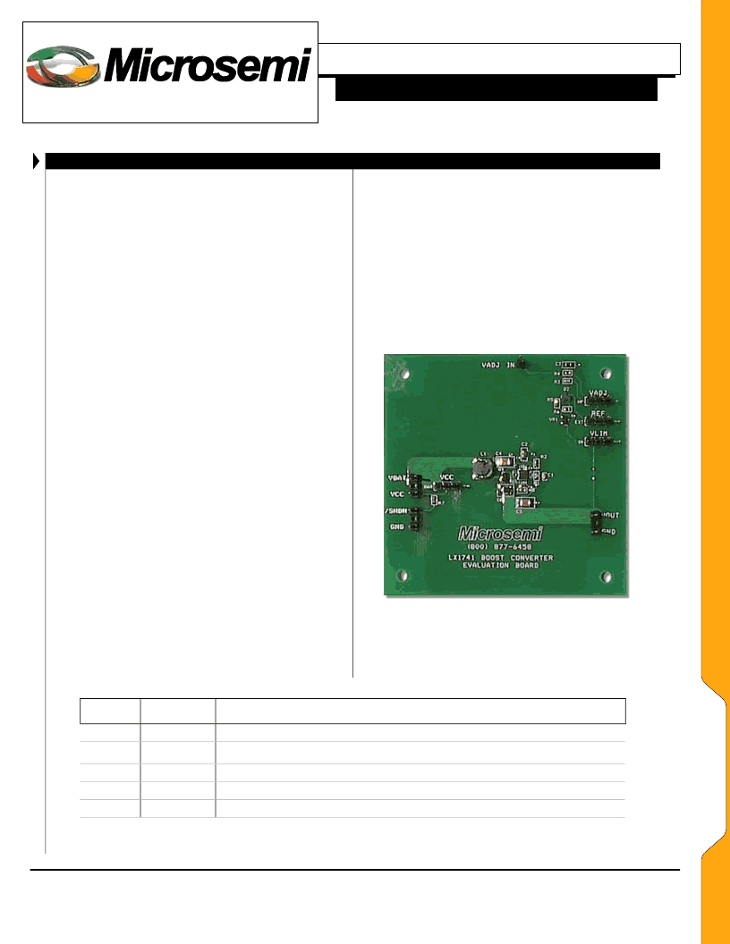
The LXE1741 evaluation board is available from
Microsemi
for assessing overall circuit performance. The
evaluation board, shown in Figure 5, is 3 by 3 inches (i.e.,
7.6 X 7.6cm) square and factory calibrated to provide a
nominal 18V output from a 1.6V to 6.0V input. Circuit
designers can easily modify output voltage and current to
suit their particular application by replacing the R1 and R
CS
values respectively. Moreover, inductor, FET, and diodes
are easily swapped out to promote design verification of a
circuit that maximizes efficiency and minimizes cost for any
particular application. The input and output connections are
described in Table 1.
E
LECTRICAL
C
ONNECTIONS
Apply the DC input voltage to VBAT (
not VCC
)
however, the LX1741 IC may be driven from a separate DC
source via the VCC input (if desired). Connect the test load
to VOUT. Primary output voltage adjustment is
accomplished by selecting the appropriate value for R1.
Optional fine adjustment of the output voltage is achieved
by applying either a DC voltage or a PWM-type signal to
the VADJ input. Both low frequency (f < 100KHz) and high
frequency (f > 100KHz) PWM signals are accommodated
by choosing the appropriate jumper connection. Further, the
VADJ circuit can be bypassed by selecting the appropriate
jumper position (see Table 2).
The LX1741 exhibits a low quiescent current (I
Q
< 1
μ
A:
typ) during shutdown mode. The SHDN pin can be used to
examine shutdown performance on the evaluation board.
This pin is pulled-up to VCC via a 10K
resistor.
Grounding the SHDN pin shuts down the IC however, the
load is still capable of drawing current through the inductor
& diode circuit path. Hence, V
OUT
during shutdown will be
approximately V
BAT
minus the inductor and diode forward
voltage drop.
The LX1741 can achieve output voltages in excess of
25V. In certain applications, it is necessary to protect the
load from excessive voltage excursions. The evaluation
board provides a VLIM jumper position for this purpose.
Engaging this jumper position ensures that the output
voltage does not exceed 25V.
The LXE1741 evaluation board provides an easy and cost
effective solution for evaluation on the LX1741. The
factory installed component list for the evaluation board is
provided in Table 3 and the schematic is shown in Figure 6.
Figure 7
– LX1741 Circuit Evaluation Board
Table 1: Input and Output Pin Assignments
Pin
Name
VBAT
Allowable
Range
0 to 6V
Description
Main power supply for output. (Set external current limit to 0.5A)
LX1741 power. May be strapped to VBAT or use a separate supply if VCC jumper is in the
SEP position.
Do not power output from VCC pin on board..
Pulled up to VCC on board (10K
), Ground to inhibit the LX1741.
VCC
1.6V to 6V
SHDN
0 to VCC
VOUT
VCC to 25V
Programmed for 18V output, adjustable up to 25V.
VADJ IN
0 to VCC
Apply a DC input or PWM input to adjust the output voltage.
Note: All pins are referenced to ground.
E
V
A
L
B
O
A
R
D
相關(guān)PDF資料 |
PDF描述 |
|---|---|
| LX1792CLM | AUDIO AMPLIFIER|SINGLE|LLCC|8PIN|PLASTIC |
| LX1810CDB | Thermo Electric Controller IC |
| LX1823 | Current-Mode SMPS Controller |
| LX1882-00CDM | Charge Pump |
| LX1882-00CDU | Charge Pump |
相關(guān)代理商/技術(shù)參數(shù) |
參數(shù)描述 |
|---|---|
| LX1741CDU-TR | 制造商:MICROSEMI 制造商全稱:Microsemi Corporation 功能描述:High Efficiency High Voltage Boost Controller |
| LX1741CLM | 功能描述:IC REG CTRLR BST PWM VM 8MLP RoHS:是 類別:集成電路 (IC) >> PMIC - 穩(wěn)壓器 - DC DC 切換控制器 系列:- 標準包裝:2,500 系列:- PWM 型:電流模式 輸出數(shù):1 頻率 - 最大:500kHz 占空比:96% 電源電壓:4 V ~ 36 V 降壓:無 升壓:是 回掃:無 反相:無 倍增器:無 除法器:無 Cuk:無 隔離:無 工作溫度:-40°C ~ 125°C 封裝/外殼:24-WQFN 裸露焊盤 包裝:帶卷 (TR) |
| LX1741CLM-TR | 制造商:MICROSEMI 制造商全稱:Microsemi Corporation 功能描述:High Efficiency High Voltage Boost Controller |
| LX1742 | 制造商:MICROSEMI 制造商全稱:Microsemi Corporation 功能描述:High Efficiency High Voltage Boost Controller |
| LX1742 EVAL KIT | 制造商:Microsemi Corporation 功能描述:EVAL KIT FOR LX1742 - Bulk |
發(fā)布緊急采購,3分鐘左右您將得到回復(fù)。