- 您現(xiàn)在的位置:買賣IC網(wǎng) > PDF目錄377793 > LX8384-XX (Microsemi Corporation) 5A LOW DROPOUT POSITIVE REGULATORS PDF資料下載
參數(shù)資料
| 型號(hào): | LX8384-XX |
| 廠商: | Microsemi Corporation |
| 英文描述: | 5A LOW DROPOUT POSITIVE REGULATORS |
| 中文描述: | 5A條陽性率低壓差調(diào)節(jié)器 |
| 文件頁數(shù): | 3/8頁 |
| 文件大小: | 216K |
| 代理商: | LX8384-XX |
5A L
OW
D
ROPOUT
P
OSITIVE
R
E G U L AT O R S
LX8384-xx/8384A-xx/8384B-xx
P R O D U C T D A T A B O O K 1 9 9 6 / 1 9 9 7
3
Copyright 1997
Rev. 1.9 12/97
P
R O D U C T I O N
D
A T A
S
H E E T
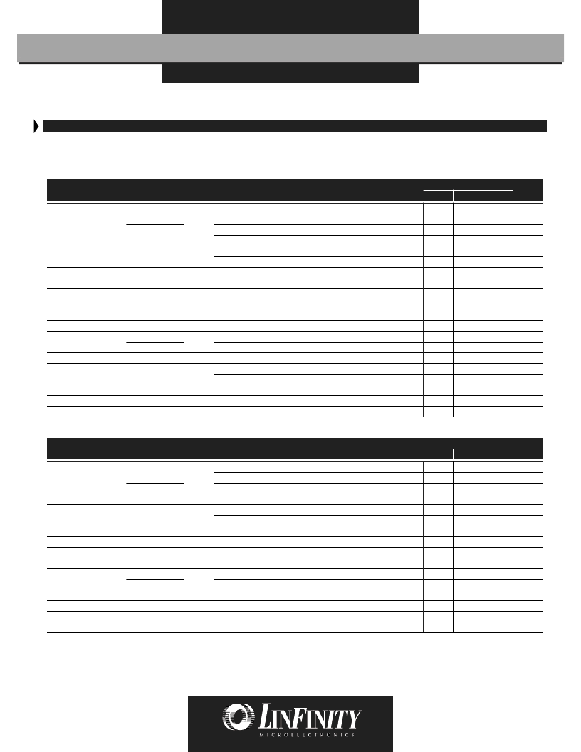
ELECTRICAL CHARACTERISTICS
(Unless otherwise specified, these specifications apply over the operating ambient temperatures for the LX8384-xxC/8384A-xxC/8384B-xxC with
0°C
≤
T
≤
125°C, and the LX8384-xxI with -25°C
≤
T
≤
125°C; V
- V
= 3V; I
OUT
= 5A. Low duty cycle pulse testing techniques are used which
maintains junction and case temperatures equal to the ambient temperature.)
LX8384-00 / 8384A-00 / 8384B-00
(Adjustable)
Parameter
Symbol
Test Conditions
Units
LX8384/84A/84B-00
Min.
Typ.
1.238
1.250
1.225
1.250
1.240
1.250
1.238
1.250
0.015
0.035
0.15
0.01
65
83
Max.
1.262
1.270
1.260
1.262
0.2
0.3
0.5
0.02
Reference Voltage
(Note 4)
LX8384/84A-00
V
REF
I
OUT
= 10mA, T
A
= 25°C
10mA
≤
I
OUT
≤
5A, 1.5V
≤
(V
IN
- V
OUT
), V
IN
≤
10V, P
≤
P
MAX
I
OUT
= 10mA, T
A
= 25°C
10mA
≤
I
OUT
≤
5A, 1.5V
≤
(V
IN
- V
OUT
), V
IN
≤
10V, P
≤
P
MAX
1.3V
≤
(V
IN
- V
OUT
), V
IN
≤
7V, I
OUT
= 10mA
1.3V
≤
(V
IN
- V
OUT
), V
IN
≤
10V, I
OUT
= 10mA
V
REF
(I
OUT
)
V
OUT
≥
V
REF
, V
IN
- V
OUT
= 3V, 10mA
≤
I
OUT
≤
5A
V
OUT
(Pwr)
T
A
= 25°C, 20ms pulse
V
OUT
= 5V, f =120Hz, C
OUT
= 100μf Tantalum, V
IN
= 6.5V
C
ADJ
= 10μF, I
OUT
= 5A
I
ADJ
I
ADJ
10mA
≤
I
OUT
≤
I
OUT (MAX)
, 1.3V
≤
(V
IN
- V
OUT
), V
IN
≤
10V
V
V
REF
= 1%, I
OUT
= 5A
V
REF
= 1%, I
OUT
= 5A
I
OUT (MIN)
V
IN
≤
10V
I
OUT (MAX)
(V
IN
- V
OUT
)
≤
7V
(V
IN
- V
OUT
)
≤
10V
V
OUT
(T)
V
OUT
(t) T
A
= 125°C, 1000 hours
T
A
= 25°C, 10Hz
≤
f
≤
10kHz
LX8384B-00
Line Regulation (Note 2)
V
REF
(V
IN
)
Load Regulation (Note 2)
Thermal Regulation
Ripple Rejection (Note 3)
Adjust Pin Current
Adjust Pin Current Change (Note 4)
Dropout Voltage
LX8384-00
LX8384A/84B-00
Minimum Load Current
Maximum Output Current
Temperature Stability (Note 3)
Long Term Stability (Note 3)
RMS Output Noise (% of V
OUT
) (Note 3) V
OUT (RMS)
V
V
V
V
%
%
%
%/W
dB
20
55
0.2
1.2
1.1
2
6
4
0.25
0.3
0.003
100
5
1.5
1.3
10
μA
μA
V
V
mA
A
A
%
%
%
5
3
1
Note 2. Regulation is measured at constant junction temperature, using pulse testing with a low duty cycle. Changes in output voltage due to
heating effects are covered under the specification for thermal regulation.
Note 3. These parameters, although guaranteed, are not tested in production.
Note 4. See Maximum Output Current Section above.
Parameter
Symbol
Test Conditions
Units
LX8384/84A/84B-15
Min.
Typ.
1.485
1.50
1.470
1.50
1.488
1.50
1.485
1.50
1
1
2.5
0.01
60
83
4
1.2
1
5
6
0.25
0.3
0.003
Max.
1.515
1.530
1.512
1.515
3
5
7
0.02
Output Voltage
(Note 4)
LX8384/84A-15
V
OUT
V
IN
= 5V, I
OUT
= 0mA, T
A
= 25°C
4.75V
≤
V
IN
≤
10V, 0mA
≤
I
OUT
≤
5A, P
≤
P
MAX
V
IN
= 5V, I
OUT
= 0mA, T
A
= 25°C
4.75V
≤
V
IN
≤
10V, 0mA
≤
I
OUT
≤
5A, P
≤
P
MAX
4.75V
≤
V
IN
≤
7V
4.75V
≤
V
IN
≤
10V
V
OUT
(I
OUT
)
V
IN
= 5V, 0mA
≤
I
OUT
≤
I
OUT (MAX)
V
OUT
(Pwr)
T
A
= 25°C, 20ms pulse
C
OUT
= 100μF (Tantalum), I
OUT
= 5A
I
Q
0mA
≤
I
OUT
≤
I
OUT (MAX)
, 4.75V
≤
V
IN
≤
10V
V
V
OUT
= 1%, I
OUT
I
OUT (MAX)
V
OUT
= 1%, I
OUT
≤
I
OUT (MAX)
I
OUT (MAX)
V
IN
≤
7V
V
OUT
(T)
V
OUT
(t) T
A
= 125°C, 1000 hours
T
A
= 25°C, 10Hz
≤
f
≤
10kHz
LX8384B-15
Line Regulation (Note 2)
V
OUT
(V
IN
)
Load Regulation (Note 2)
Thermal Regulation
Ripple Rejection (Note 3)
Quiescent Current
Dropout Voltage
LX8384-15
LX8384A/84B-15
Maximum Output Current
Temperature Stability (Note 3)
Long Term Stability (Note 3)
RMS Output Noise (% of V
OUT
) (Note 3) V
OUT (RMS)
V
V
V
V
mV
mV
mV
% / W
dB
mA
V
V
A
%
%
%
10
1.5
1.3
1
LX8384-15 / 8384A-15 / 8384B-15
(1.5V Fixed)
相關(guān)PDF資料 |
PDF描述 |
|---|---|
| LX8384-00CDD | 5A LOW DROPOUT POSITIVE REGULATORS |
| LX8384-00CP | 5A LOW DROPOUT POSITIVE REGULATORS |
| LX8384-00IDD | 5A LOW DROPOUT POSITIVE REGULATORS |
| LX8384-00IP | 5A LOW DROPOUT POSITIVE REGULATORS |
| LX8384B-33CDD | 5A LOW DROPOUT POSITIVE REGULATORS |
相關(guān)代理商/技術(shù)參數(shù) |
參數(shù)描述 |
|---|---|
| LX8384-XXCDD | 制造商:MICROSEMI 制造商全稱:Microsemi Corporation 功能描述:5A Low Dropout Positive Regulators |
| LX8384-XXCDD-TR | 制造商:MICROSEMI 制造商全稱:Microsemi Corporation 功能描述:5A Low Dropout Positive Regulators |
| LX8384-XXCDT | 制造商:MICROSEMI 制造商全稱:Microsemi Corporation 功能描述:5A Low Dropout Positive Regulators |
| LX8384-XXCDT-TR | 制造商:MICROSEMI 制造商全稱:Microsemi Corporation 功能描述:5A Low Dropout Positive Regulators |
| LX8384-XXCP | 制造商:MICROSEMI 制造商全稱:Microsemi Corporation 功能描述:5A Low Dropout Positive Regulators |
發(fā)布緊急采購,3分鐘左右您將得到回復(fù)。