- 您現(xiàn)在的位置:買賣IC網(wǎng) > PDF目錄376118 > LXMG1643-12-62 (Microsemi Corporation) 12V Quad 6W CCFL Programmable Inverter Module PDF資料下載
參數(shù)資料
| 型號: | LXMG1643-12-62 |
| 廠商: | Microsemi Corporation |
| 英文描述: | 12V Quad 6W CCFL Programmable Inverter Module |
| 中文描述: | 12V的可編程四6W冷陰極逆變器模塊 |
| 文件頁數(shù): | 5/6頁 |
| 文件大小: | 200K |
| 代理商: | LXMG1643-12-62 |

P
RODUCTION
D
ATA
S
HEET
Microsemi
Integrated Products
11861 Western Avenue, Garden Grove, CA. 92841, 714-898-8121, Fax: 714-893-2570
Page 5
Copyright
2005
Rev. 1.1, 2006-11-16
W
M
.
C
P
P
a
a
n
n
e
e
l
l
M
a
a
t
t
c
c
h
h
LXMG1643-12-62
12V Quad 6W CCFL Programmable Inverter Module
TM
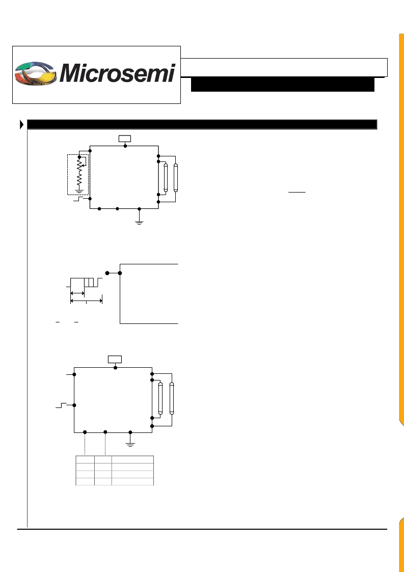
T Y P I C A L A P P L I C A T I O N
LXMG1643-12-62
12V
SET
2
GND
V
Hx
V
LOx
BRITE
V
IN1
SLEEP
SET
1
0.45V
to 2.0V
1.8K
20K
DAC or
Pot
NC
NC
V
Hx
One of two
V
LOx
Figure 1
– Brightness Control
(Output current set to maximum)
PWM Signal
from System
P.W.
10μs to 125μS
BRITE
LXMG1643-12-62
0 < P.W. < 100% of period
Figure 1A
– PWM Brightness Control
LXMG1643-12-62
SLEEP
BRITE
12V
V
IN1
SET
2
GND
SET
1
One
of two
L
L
H
H
L
H
L
H
5.0mA
RMS
6.0mA
RMS
7.0mA
RMS
8.0mA
RMS
L=GND; H=Open
Figure 2
– Maximum Output Current
(SET
1
and SET
2
Inputs)
The brightness control may be a voltage output DAC or
other voltage source, a digital pot or 20K manual pot. The
inverter contains an internal 10K pull-up to 3V to bias the
pot add a 1.8K resistor to set the lower threshold voltage.
A 3.3V Logic Level PWM signal from a micro-controller
may also be used as shown in Figure 1A.
If you need to turn the inverter ON/OFF remotely, connect
to TTL logic signal to the
SLEEP
input.
Connect V
HI
to high voltage wire from the lamp. Connect
V
LO
to the low voltage wire (wire with thinner insulation).
Never connect V
LO
to circuit ground as this will defeat
lamp current regulation. If both lamp wires have heavy
high voltage insulation, connect the longest wire to V
LO
.
This wire is typically white.
Use the SET
1
and SET
2
(see Figure 2) inputs to select the
desired maximum output current. Using these two pins in
combination allows the inverter to match a wide variety of
panels from different manufactures. Generally the best
lamp lifetime correlates with driving the CCFL at the
manufactures nominal current setting. However the SET
1
and SET
2
inputs allow the user the flexibility to adjust the
current to the maximum allowable output current to
increase panel brightness at the expense of some reduced
lamp life.
Although the SET pins are designed such that just leaving
them open or grounding them is all that is needed to set the
output current, they can also be actively set. Using an open
collector or open drain logic signal will allow you to
reduce the lamp current for situations where greater dim
range is required, as an example in nighttime situations. In
conjunction with a light sensor or other timer the panel
could be set to higher brightness (maximum output
current) for daytime illumination and lower brightness
(minimum or typical output current) at nighttime. Since
the dim ratio is a factor of both the burst duty cycle and the
peak output current, using this technique, the effective dim
ratio can be increased greater than the burst duty cycle
alone. Conversely the SET inputs could be used to
overdrive the lamp temporarily to facilitate faster lamp
warm up at initial lamp turn on. Of course any possible
degradation on lamp life from such practices is the users
responsibility since not all lamps are designed to be
overdriven.
The inverter has a built in fault timeout function. If the
output return is open (lamp disconnected or broken) or
shorted the inverter will attempt to strike the lamp for
several seconds. After about a second without success the
inverter will shutdown. In order to restart the inverter it is
necessary to toggle the sleep input or cycle the V
IN1
input
supply. In the timeout shutdown mode input drain current
will be about 8mA.
A
P
P
L
I
C
A
T
I
O
N
S
相關(guān)PDF資料 |
PDF描述 |
|---|---|
| LXMG1643-12-63 | 12V Quad 6W CCFL Programmable Inverter Module |
| LXMG1643-12-64 | 12V Quad 6W CCFL Programmable Inverter Module |
| LXMG1644-12-61 | 12V Quad 6W CCFL Programmable Inverter Module |
| M-201-T | High flow,adjustable flow switch with right-angle flow |
| M-201xxx | SUBMINATURE/MULTI-FUNCTION/UNBRACKETED |
相關(guān)代理商/技術(shù)參數(shù) |
參數(shù)描述 |
|---|---|
| LXMG1643-12-63 | 功能描述:12V QUAD CCFL PROGRAM INVERT MOD RoHS:否 類別:光電元件 >> 反相器 系列:LXMG1643-12-6x 標準包裝:100 系列:- 輸入電壓:6.0V 輸出:900V 類型:用于 CCFL 和 UV 燈的逆變器 尺寸/尺寸:2.34" L x 0.35" W x 0.35" H(59.5mm x 9mm x 8.9mm) 安裝類型:底座安裝 |
| LXMG1643-12-64 | 功能描述:MOD INVERTER CCFL QUAD 6W 12V RoHS:是 類別:光電元件 >> 反相器 系列:PanelMatch™ 標準包裝:100 系列:- 輸入電壓:6.0V 輸出:900V 類型:用于 CCFL 和 UV 燈的逆變器 尺寸/尺寸:2.34" L x 0.35" W x 0.35" H(59.5mm x 9mm x 8.9mm) 安裝類型:底座安裝 |
| LXMG1644-12-61 | 功能描述:MOD INVERTER CCFL QUAD 6W 12V RoHS:是 類別:光電元件 >> 反相器 系列:LXMG1644-12-6x 標準包裝:100 系列:- 輸入電壓:6.0V 輸出:900V 類型:用于 CCFL 和 UV 燈的逆變器 尺寸/尺寸:2.34" L x 0.35" W x 0.35" H(59.5mm x 9mm x 8.9mm) 安裝類型:底座安裝 |
| LXMG1645-12-51 | 制造商:MICROSEMI 制造商全稱:Microsemi Corporation 功能描述:12V Quad 5W CCFL Inverter Module |
| LXMG1645-12-52 | 制造商:MICROSEMI 制造商全稱:Microsemi Corporation 功能描述:12V Quad 5W CCFL Inverter Module |
發(fā)布緊急采購,3分鐘左右您將得到回復(fù)。